Definition: The Sample and Hold circuit is an electronic circuit which creates the samples of voltage given to it as input, and after that, it holds these samples for the definite time. The time during which sample and hold circuit generates the sample of the input signal is called sampling time. Similarly, the time duration of the circuit during which it holds the sampled value is called holding time.
Sampling time is generally between 1µs to 14 µs while the holding time can assume any value as required in the application.
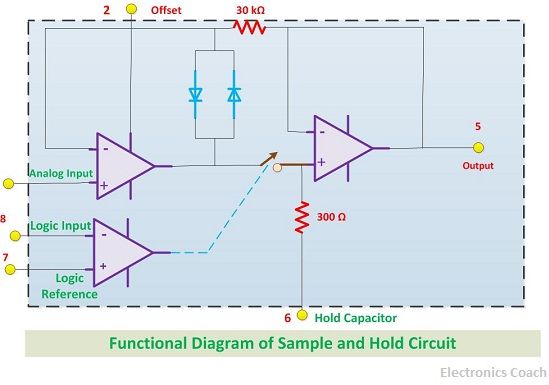
It will not be wrong to say that capacitor is the heart of sample and hold circuit. This is because the capacitor present in it charges to its peak value when the switch is opened, i.e. during sampling and holds the sampled voltage when the switch is closed.

Circuit Diagram of Sample and Hold Circuit
The diagram below shows the circuit of the sample and hold circuit with the help of an Operational Amplifier. It is evident from the circuit diagram that two OP-AMPS are connected via a switch. When the switch is closed sampling process will come into the picture and when the switch is opened holding effect will be there.
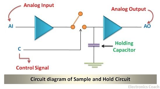
The capacitor connected to the second operational amplifier is nothing but a holding capacitor.
Significance
Now, you all are aware that what is the sample and hold circuit. But what are the driving forces which have turned us in the direction to use the sample and hold circuit? To understand this, we need to enter into communication realm. We all know digital communication is better than analogue communication, but why? What is wrong with analogue communication?
The noise interference is the real culprit. It makes analogue communication less efficient and less reliable. Thus, in digital communication, we need digital signals. But naturally, all the signals are analogue. This is the turning point where we need a sample and hold circuit.
With the help of sample and hold circuit we can take samples of the analogue signal, followed by a capacitor. It holds these sample for a particular period. As a consequence of this, a constant signal is generated this can be converted into the digital signal with the help of analogue to digital converters.
Working of Sample and Hold Circuit
The working of sample and hold circuit can be easily understood with the help of working of its components. The main components which a sample and hold circuit involves is an N-channel Enhancement type MOSFET, a capacitor to store and hold the electric charge and a high precision operational amplifier.
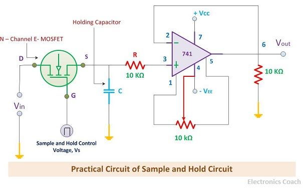
The N-channel Enhancement MOSFET will be used a switching element. The input voltage is applied through its drain terminal and control voltage will be applied through its gate terminal. When the positive pulse of the control voltage is applied, the MOSFET will be switched to ON state. And it acts as a closed switch. On the contrary, when the control voltage is zero then the MOSFET will be switched to OFF state and acts as the open switch.
When the MOSFET acts as a closed switch, then the analogue signal applied to it through the drain terminal will be fed to the capacitor. The capacitor will then charge to its peak value. When the MOSFET switch is opened, then the capacitor stops charging. Due to the high impedance operational amplifier connected at the end of the circuit, the capacitor will experience high impedance due to this it cannot get discharged.
This leads to the holding of the charge by the capacitor for the definite amount of time. This time can be referred as holding period. And the time in which samples of the input voltage is generated is called sampling period.
The output processed by operational amplifier during the holding period. Therefore, holding period holds significance for OP-AMPS.
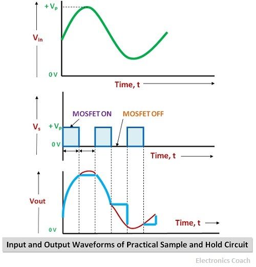
Input and Output Waveforms
The waveforms as described in the diagram clearly depicts the picture. It is evident from the waveform of the sample and hold circuit, that during the ON duration what will be the voltage at the output. During the OFF duration the voltage that exists at the output of OP-AMP.
Connections
The connection diagram helps us to build a better understanding about the input voltage and control voltage and how they are applied to the OP-AMP. The capacitor used should be versatile so that it does possess any leakage. The capacitor made of Teflon and polyethylene will be appropriate to achieve our desired purpose.
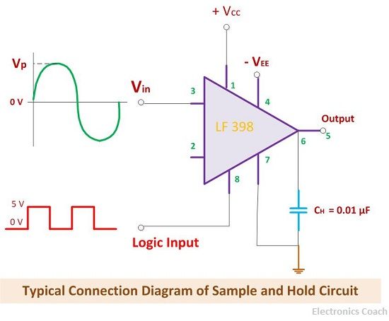
In the connection diagram, you can see that LF 398 is written, that is nothing but the special architecture IC for sample and hold circuit.
The crucial point to be noted here is the frequency of analog input signal and control signal. To maintain the efficiency of the sample and hold circuit it is very important to observe the frequency. The frequency of the control voltage should be greater than the frequency of input voltage so that the analog signal can be sampled twice in a complete cycle.
Functional diagram
With the help of this diagram, we can easily interpret that how a sample and hold circuit functions.
Performance Parameters
- Acquisition Time (TAC): The time required by the capacitor to get the charge of the input voltage applied to the sample and hold circuit. It is referred as acquisition time.
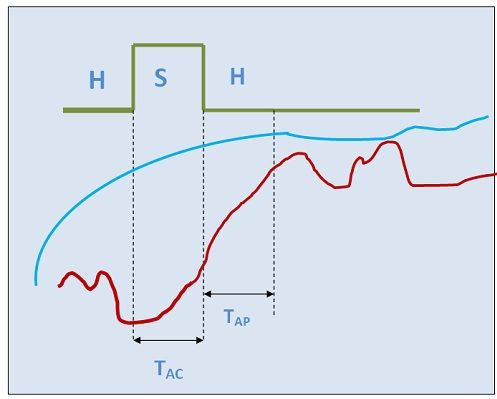
- Aperture Time (TAP): The aperture time can be defined as the time required by the capacitor to change its state from sampling to holding. Due to the propagation delay of switches, even after the hold command is given the capacitor still keeps on charging for the short duration of time. This is nothing but aperture time.
- Voltage Droop: The voltage droop is the voltage drop down in the capacitor due to leakage of charge by a capacitor. Ideally, we require capacitors which do not possess any leakage, but it is not possible practically. No matter how good quality material we use there will be some voltage drop.
- Hold Mode Settling Time: After the generation of hold commands, the analogue input voltage which is used by the capacitor for charging takes some time to settle completely. This is called Hold Mode settling time.
Application of Sample and Hold Circuit
- Data Distribution System
- Sampling Oscilloscopes
- Data Conversion System
- Digital Voltmeters
- Analog Signal Processing
- Signal Constructional Filters
This completes the detailed description of the sample and hold circuit. Thus, in simple terms sample and hold circuit generates the samples of the analogue input signal and holds the latest sampled values for definite time and reflects it at the output.
G.T says
Suppose that capacitor is holding a sampled value . What will happen when next sample value is applied to it ? ..can you please elaborate the working using fig.2 …
Krati P says
Please look at diagram 2, in this it has two operational amplifiers, when the control signal is applied then the switch will be closed and the sampling process prevails but when the switch is opened no more sampling can be done because circuit is not complete due to open switch, then the capacitor will hold the previously sampled values. Remember, the control signal here is crucial it will be controlled as per the requirement of sampling or holding.
Hope it will help, in case of more queries, feel free to ask.
Kavita says
Nicely explained thanks
Krati P says
Thanks for the appreciation !!!
Pavani says
At the terminal. 2 of Ic398 we use 47k resistor connected to ground. What is the reason behind it???
KOKKERLAPATI KRISHNAMRAJU . says
awesome mam…thank you so much.