The crucial difference between BJT and JFET is that BJT is a bipolar device while JFET is a unipolar device. It is so because the operation of BJT is dependent on injection and collection of minority charge carriers that includes both electrons and holes. As against JFET is majority carrier device, thus termed as unipolar.
Another major difference between BJT and JFET is that BJT falls under current controlled device category whereas JFET falls under voltage controlled device category.
We will discuss some other major differences between BJT and JFET but before proceeding further have a look at the contents to be discussed under this article.
Content: BJT Vs JFET
Comparison
| Parameter | BJT | JFET |
|---|---|---|
| Carrier | Bipolar (majority and minority) | Unipolar (majority) |
| Symbol | 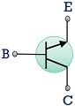 | 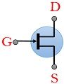 |
| Device type | Current controlled device. | Voltage controlled device. |
| Input impedance | Low | High |
| Gain | High gain | Low - medium gain |
| Power consumption | It consumes more power. | It consumes less power. |
| Noise level | High | Low |
| Thermal stability | Low | High |
| Size | Large | Small |
| Application preference | It is preferred in low current application. | It is preferred in low voltage application. |
Definition
BJT
BJT is the short form used for bipolar junction transistor. It is a 3 terminal device that is used for switching or amplification purpose.
The figure below shows the basic construction of a bipolar transistor consisting of 3 terminals emitter, base and collector.
It is formed by fusing two p-n junction diodes, that shares a common terminal. The common terminal can be either p or n as we can see in the figure shown above.
It is a current regulating device which controls the current flowing through it. There exist two different configurations of a BJT, i.e., NPN or PNP. Both hold the same operating principle but the difference between the two is their biasing and polarity of power supply voltage.
Let’s have a look at the basic operation of NPN bipolar transistor.
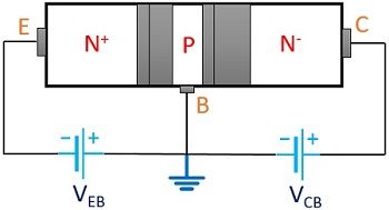
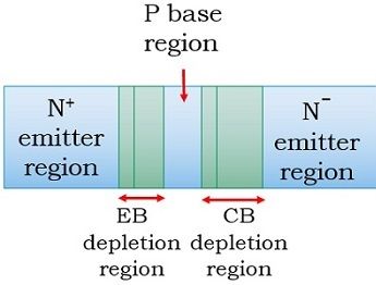
In normal operating conditions, EB junction is always forward biased whereas CB junction is always reverse biased as we can see in the figure shown above.
Due to the forward applied voltage VEB, the electrons in the N region experiences repulsive force and drifts across the lightly doped base region after overcoming the barrier potential. As the base region is lightly doped, only some of the drifted electrons recombine with the holes in the base region.
Now, the increased concentration of electrons in the base region causes more electrons to move across the collector region. As this region is reversed biased, the electrons are immediately collected by this region.
Thus, a proper flow of current is noticed and hence the emitter current is the summation of base and collector current.
JFET is the short form used for Junction Field Effect Transistor. It is a 3 terminal unipolar device that controls the flow of current through the device by the applied input voltage. Here, the 3 terminals are termed as the source, gate and drain.
It is known so because the output current of the device is controlled by the field associated with depletion region.
It can be either n channel JFET or p channel JFET.
As it is a voltage controlled device thus the applied input potential allows the movement of electrons hence causing current to flow through the device.
The figure below shows an n channel JFET with the positive voltage at the drain terminal.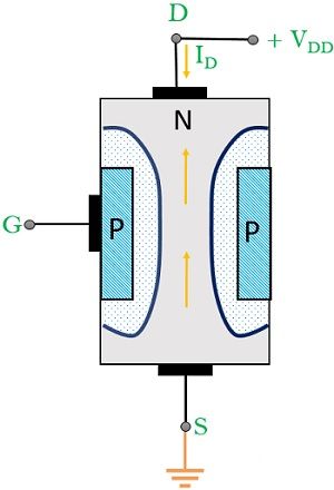
In the absence of any applied input voltage, the two depletion region around the PN junctions is equally wide and symmetrical. However, on applying a positive potential to the drain wrt source, electrons start flowing from source to drain. Thus, causing the drain current to flow through the drain to source.
Another condition exists when the gate terminal is applied with negative potential and drain is positively biased as we can see below:
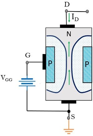
This reverse biasing of the p-n junction allows a considerable increase in the width of the depletion region. Resultantly, this narrows the channel length and drain current is decreased due to an increase in resistance.
Any additional increase in the gate voltage will cause the drain current to cut-off completely. Conversely, by lowering the negative biasing of the gate terminal, the width of the depletion region reduces.
Key Differences Between BJT and JFET
The points given below describes the difference between BJT and JFET:
- The key difference between BJT and JFET is that BJT is a device in which output current is controlled by the base current. On the contrary, JFET is a device whose output current is controlled by the input voltage applied to it.
- BJT possess low to medium input impedance whereas when we talk about JFET, it possesses high input impedance.
- Whenever there is a need for high gain and fast response then BJT’s are preferred while JFET’s are low gain devices.
- A BJT is a device that possesses low thermal stability whereas JFET possesses high thermal stability.
- Another key difference that exists between BJT and JFET is that BJT is preferred in low current applications while JFET is preferred in low voltage applications.
Conclusion
Although both BJT and JFET belong to transistor family, their operating principle differentiates the two. The larger size of BJT and more power consumption as compared to JFET sometimes proves as its disadvantage.
Leave a Reply