We are already aware of JFETs; now we should be acquainted with its application in electronics realm. An amplifier is one of the most significant electronic devices which is used in almost every domain whether it is communication system or power systems. In the same way, by which we use bipolar transistors as an amplifier, we can also utilize JFET as an amplifier.
Using JFET as an amplifier
To understand, how a JFET works as an amplifier, first we should be well aware of the fact that how does an amplifier work. It takes an input signal which is weak in magnitude and amplifies it by its internal circuit. The weak signal applied at its input circuit causes a large change in its output circuit.
The load resistor is used to reflect this large change which causes the large voltage drop across the load resistor, and thus, a large current is received at the output terminal.
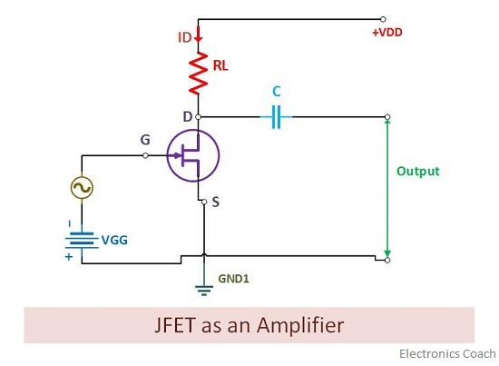
Now, let’s understand this concept with the help JFET. But before that have a quick look at its circuit. It consists of N-channel JFET, a capacitor, AC signal input, a load resistor and battery to supply gate to source voltage. More precisely, the battery here is used for providing a reverse bias to the input circuitry.

Working
The working procedure of JFET as an amplifier can be easily conceived even if we know a little about vacuum tube. In case of a vacuum tube, we supply the weak input signal between its grid and cathode. This creates a large change in the output obtained at plate circuit. This large change is a desired feature here. This is something which creates an amplifier.
Now, let’s come back to JFET. The gate and source terminal is connected to the battery in such a way that gate terminal is connected to the negative terminal of the battery and source terminal is connected to the positive terminal of the battery. This is because we need to reverse bias the input circuitry of JFET.
The input signal which is weak in magnitude is applied by AC signal source. It is supplied as alternate positive, negative half cycles of AC. When the AC signal is applied to the input circuitry, it will start altering the gate to source voltage.
It will have two effects on the gate to source voltage, either it will reduce the magnitude of reverse biasing applied to the gate-source terminal, or it will increase the reverse biasing of the gate to the source terminal.
Reduced Gate Source reverse voltage
If the reverse voltage falls down, then the width of the depletion region inside the channel will starts decreasing. We have already discussed in our previous article that if the width of the depletion region starts decreasing, then the channel width will be increased. Consequently, the magnitude of charge carriers (Electrons in case of N-channel JFET) flowing from source to drain will increase.
This will directly contribute to increase in the drain current. The load resistor is connected to the output circuit. The current flowing through it will create a voltage drop, and thus large current will flow through it. This leads to amplification of the signal. And thus JFET as an amplifier is designed.
Increase in reverse voltage at gate-source terminal
If the AC signal applied at the input terminal will increase the reverse voltage, then the width of the depletion region will start increasing. Due to this, the drain current will starts decreasing. And again the small change in input will cause a large change across the load resistor. This performs the amplification action in JFET.
Performance Parameters of JFET
- AC Drain Resistance: The ratio of change in voltage across the drain-source terminal and the change in drain current is termed as AC drain resistance. But the ratio should be considered at a point when the gate-source voltage is kept constant. Its value is in range of 10 kΩ to 1 MΩ. It is also referred as dynamic resistance (rd), it should not be confused with the resistance of channel (RDS), Rds is purely DC while rd is not.

- DC Drain Resistance: RDS is a symbol used for DC drain resistance. It is the ratio between the change in drain-source voltage and the change in drain current. The value of DC drain resistance is static. Thus it is also termed as static or ohmic resistance.

- Transconductance: It is the ratio between the change in drain current and the change in gate-source voltage but at constant drain-source voltage. It is represented by gm.

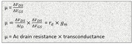
- Amplification factor: The amplification factor is obtained by determining the ratio between the change in drain-source voltage with respect to change in gate-source voltage but keeping the value of drain current constant.

It is represented by µ. The value of amplification factor can be high as 100.

The Significance of the amplification factor is that it helps to determine the control of gate to source voltage on the value of drain current in comparison to that of the drain to source voltage.
Stephen says
Clear explanation, thank you