Definition: JFET is an acronym used for Junction field effect transistor. The JFET works on the principle that the current, more precisely the output current which flows through the device varies with the applied gate voltage.
Thus, the electric field applied at gate terminal control the flow of current through the device and thus its name is field effect transistor.It consists of three terminals that are gate, source and drain.
The output current flows from the drain terminal towards the source terminal. Therefore, the output current is termed as the drain current. To understand the working characteristics of JFET we need to consider one type of JFET either N-channel JFET or P-channel JFET.
The difference between these two JFETs is the current carriers involved in the conduction mechanism. The N-channel involves the conduction due to the flow of electrons while the P-channel JFET involves conduction due to holes.
Working of JFET
Its working can be easily understood with the help of three cases. Let’s understand it one by one.
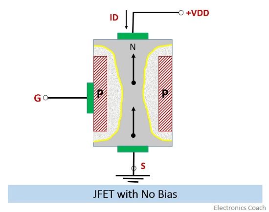
- When NO bias is applied: In this case, no bias is applied to the gate terminal. It means the gate to source voltage (Vgs) in this case is 0. Besides, the voltage at drain terminal is also 0. In this case, the width of depletion region will remain constant. The electrons will flow from source terminal to gate terminal.

The direction of flow of current is opposite to the direction of flow of electron. Thus, current will flow from drain to source terminal. The ohmic contacts are made at drain, gate and source to provide the connection.
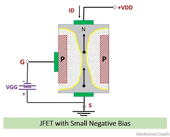
- When small negative bias is applied: When a small negative voltage is applied to the gate terminal i.e. when the gate to source voltage is negative, then the width of depletion region starts increasing.
Simultaneously, the positive voltage is applied to the drain to the source terminal. The N-channel is moderately doped while P-channel is highly doped. Due to this the width of the depletion region is more in N-Channel than in P-channel.

The wedge shape depletion layer so formed will reduce the magnitude of the current through the N-channel. This is because as the width of the depletion layer increases the space provided for electrons to flow from source to drain will decrease and eventually the drain current decreases.
The width of the depletion region is more near the drain terminal and less near the source terminal. This is because the gate is more negative at the points which are nearer to drain than to source. Besides, the current flowing from drain to source flows from the region of high resistance to low resistance, thus the voltage drop will be created.
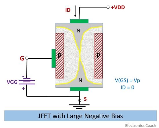
- When the Large negative bias is applied: When the large negative gate to source voltage is applied, then this large negative electric field will contribute to increment of the width of the depletion region.
The negative voltage at gate terminal implies that the P-terminal is connected to negative terminal of battery while N terminal is connected to the positive terminal. This forms the reverse biased PN junction.

The reversed biased PN junction will create the depletion region and more the reverse voltage more will be the width of the depletion region. Thus, at a certain point of negative voltage, a point will reach when the drain current completely cuts off, and the depletion layer from both the sides will almost touch each other at region nearer to drain terminal.
This point of voltage is called pinch-off voltage. Thus, the Pinch-off voltage can be defined as the reverse voltage applied at the gate to source terminal such that the drain current will cease completely. At this point of time, no current will flow from the junction field effect transistor.
Merits of JFET
- JFET has a longer life and high efficiency because of its simple construction and fabrication.
- It possesses high input impedance in order of 100 MΩ, this is because the circuit which is at the input side of JFET is reverse biased. Due to this reverse biasing the JFET provides a much higher degree of isolation between input circuit attached to it and the output circuit connected to it.
- Due to its unipolar nature, it is easy to operate. It involves either electrons or holes for conduction. At a time only one type of charge carrier is involved in the conduction mechanism which makes it simpler.
- It possesses better thermal stability this is because the negative temperature coefficient which its resistance possesses.
- The frequency response offered by JFET is also very high.
Demerits of JFET
- The JFETs are expensive and required to be handled carefully. It is more vulnerable to damage than ordinary transistors.
- It possesses low voltage gains and small trans-conductance.
- The gain-bandwidth product of JFETs is also small.
This is all about merits and demerits of JFET. Although it consists of some drawbacks but it is still a significant electronic device. It has both pros and cons but former outweighs the later.
Leave a Reply