Definition: Insulated Gate Bipolar Transistor is a voltage-controlled ideal switching device formed by the combination of BJT and MOSFET. The IGBT utilizes the best qualities of BJT and PMOSFET to generate a transistor that possesses input characteristics of MOSFET and output characteristics of BJT.
It is regarded as an advancement of power MOS technology and is abbreviated as IGBT but sometimes called as MOSIGT i.e., Metal Oxide Semiconductor Insulated Gate Transistor, COMFET i.e., Conductively Modulated Field Effect Transistor or GEMFET i.e., Gain Modulated Field Effect Transistor.
Symbolically IGBT is represented as: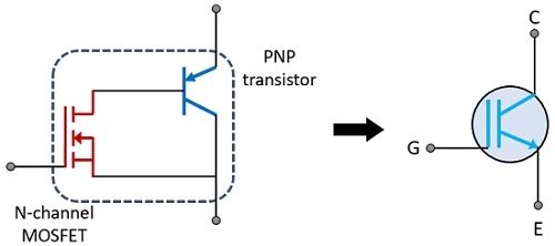
The three terminals of IGBT are emitter, collector, and gate.
Introduction to IGTB
We have already discussed in the beginning that IGBT is a combination of MOSFET and BJT which is used as an electronic switch that offers fast switching characteristics with high efficiency. The combination of MOSFET and BJT acts in IGBT in a way that the input characteristics are due to MOSFET and the output characteristics are because of BJT. In IGBT, MOSFET offers high value of input impedance with fast switching speed while BJT offers low saturation voltage.
More simply, we can say, that the IGBT is a device designed with the aim to provide high input impedance like a PMOSFET whereas low on state power loss similar to BJT. BJT suffers from a second breakdown issue which is not present in IGBT.
Structure
To construct IGBT a single silicon chip is considered over which multiple structural cells are connected in a proper manner. The basic structural representation of IGBT is given below: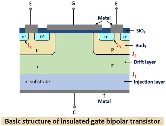
From the figure given here, it is clear that the construction of IGBT is similar to that of power MOSFET with a difference in the substrate used. The difference is that in PMOSFET, n+ substrate layer is used which is replaced by a p+ layer referred to as collector C. This p-type substrate that forms a connection with the collector terminal is known as the injection layer as it provides majority carriers i.e., holes to the n- layer whose thickness is directly proportional to the voltage blocking capability of the device.
The p-layer present here forms the body of the IGBT. So, here pn– is regarded as junction J2.
It is clear from the above figure that the structure is vertically oriented so as to attain the maximal value of current flowing through the device. Here, we have constructed an n channel IGBT but by changing the doping type we can form a p channel IGBT.
Equivalent Circuit
The figure below represents the equivalent circuit of IGTB formed by considering the above given basic structure: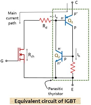
Working of IGBT
Let us now understand how an IGTB operates:
Initially, the device is forward biased by making the collector terminal positive with respect to the emitter terminal. Also, there is null voltage between the gate and emitter terminal thus the junctions between the p region and n– region i.e., J2 will be reverse biased. So, under the reverse biased condition, no flow of current through the device will take place.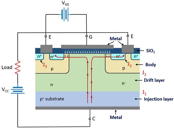
Furthermore, when a positive voltage is provided at the gate with respect to the emitter then if VG becomes greater than the threshold value of IGTB then this will result in the formation of n channel i.e., inversion layer in the p region beneath the gate like the one which is formed in MOSFETs. The formation of the channel resultantly short-circuited the n+ emitter region with the n– drift region. Hence, now through this n-channel, electrons start flowing from the n+ emitter region to the n– drift region.
Also, due to the forward biased condition of the collector-emitter terminal, holes from the p region start flowing into the n– drift region. This resultantly floods the n– drift region with both electrons and holes coming from the p body region and the p+ collector region respectively. Thus, the injection carrier density at the n- drift region gets increased by a considerable amount resultantly increasing the conductivity. This allows conduction within the IGBT as the flow of charged carriers resultantly causes the flow of collector current IC through the device and it gets turned on.
It is clear from the above discussion that the collector current is the result of injected holes from the p+ region towards the n–p i.e., transistor Q1 with resistance Rby and injected electrons from p+ collector to the n– drift region with n channel resistance Rch.
Thus,
IC = IE = Ih + Ie
On writing the respective voltage drop we will get,
VCE.on = IC. Rch + IC.Rd + Vj1
For pn junction diode Vj1 exists between 0.7 to 1V.
Characteristics of IGBT
The figure below represents the static I-V characteristics of n channel IGBT: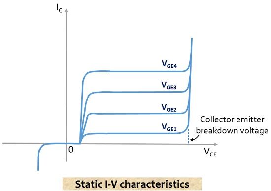
From the above-given graphical representation, it is clear that we have plotted the curve between collector current IC and collector-emitter voltage VCE for different values of gate emitter voltage VGE. This signifies that the IGTB is a voltage-controlled device.
In the absence of gate emitter voltage, then due to the reverse biased condition of junction J2 no current flows through the device. When gate emitter voltage is provided to the IGTB, then even if the supplied voltage is less than the threshold value then also, no flow of current will take place through the device thus it is in the off-state. But for various values of VGE above the threshold different current flows through the device.
Advantages
- It offers fast switching speeds.
- The on-state resistance is quite low.
- It possesses high voltage capability.
- Bipolar in nature thus offers increased conduction.
- Lower switching losses are associated with it.
- It offers more efficiency than BJT and MOSFET.
Disadvantages
- It offers a comparatively higher turn-off time than MOSFETs.
- Latch-up issue can cause excessive power dissipation of the device leading to destroy it.
Applications of IGBT
These generally find applications in devices that require medium power for their operation such as UPS system, power supplies, ac as well as dc motor drives, in driving solenoids, contractors, etc.
Leave a Reply