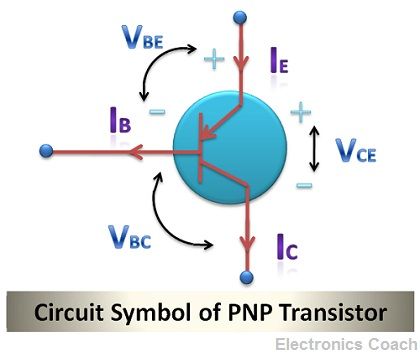
Definition: PNP transistor is three terminal current controlled device which consists of three terminals formed by sandwiching a layer of N-type material between the two P-type semiconductors. It acts as a current sink because all the emitter current sinks into the base terminal.
PNP transistor can also be understood as positive – negative – positive transistor.
The majority charge carriers involved in the conduction process of PNP transistor are holes. Thus, the current which generates at the collector is the consequence of the movement of holes.

You must be thinking how the flow of holes results in the flow of current in the circuit. You will understand this concept in the working which I will be discussing later in this article. Before that, let’s discuss its construction.
Construction
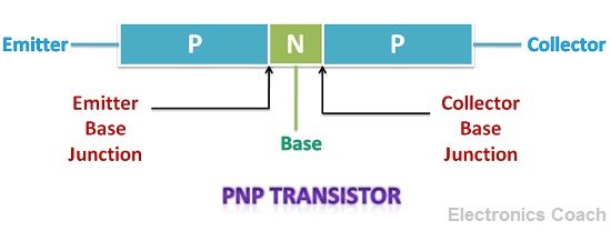
The PNP transistor is formed three layer of semiconductor, one is N-type and other two are P-type. The structure thus formed will be a PNP transistor. It will have three terminal, the first P-type semiconductor is called emitter and the other P-type material is termed as the collector.
The semiconductor material which is between both this semiconductor is called base terminal. The PNP transistor is biased in such a way that the base-emitter junction is forward biased and collector based junction is reversed biased.

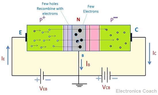
Therefore, the emitter terminal is connected to the positive terminal of the battery VEB while the base terminal of the transistor is connected to a negative terminal of the battery VEB. The collector based junction is reversed biased by connecting the collector terminal with the negative terminal of the battery VCB while the base terminal is connected to positive terminal of the battery VCB.
The magnitude of the voltage of the battery which is used to bias emitter and base terminal of the transistor is more as compared with the battery source which is used to bias the collector base terminal of the battery source.
Working of PNP Transistor
PNP transistor works when the emitter-base junction is forward biased while collector-base junction is reverse biased. The emitter terminal is formed by P-type semiconductor thus, for forward biasing the P-type terminal should be connected with positive terminal and N-type with negative terminal.

Similarly, in order to reverse bias collector-base junction, the P-type is connected with negative terminal while the N-type is connected with positive terminal.
After applying biasing the depletion region formed at the emitter-base junction will be narrow while the depletion region formed at the collector-base junction will be wide. This is because emitter-base junction is forward biased and in forward biased the depletion layer in narrow. Therefore, due to reverse biasing of collector-base junction the depletion width is broad.
Concept of Effective base width
The holes are the majority charge carrier in P-type semiconductor and electrons are the majority charge carriers in N-type electrons. The hole in emitter region will be repelled by the positive terminal of the battery and will be attracted by electrons present in the N-region. Thus, the effective base width between both the junctions will be reduced.
Effective of Doping and Size of Enmitter
We have already discussed in our previous article that the emitter is heavily doped than base and collector and area of the emitter is also more than the base but less than the collector. The base is lightly doped so it has fewer electrons.
As a consequence of which these few electrons will combine with holes emitted from emitter region due to repulsion from the positive terminal of the battery. But only a few holes will combine with electrons present in the base region due to the small size of the base and light doping.
The majority of electrons are remaining that has not combined with electrons of base terminal. These electrons will flow towards collector. They will further move towards the end of collector region because they are attracted by negative terminal of the battery through which collector is connected.
In this due to movement of holes, electric current flows in the circuit. Some of the holes also away from base constituting the base current in the circuit.
The direction of current flowing in the emitter will be towards emitter while the direction of current flowing in base and collector will be outwards. The equation of current in PNP transistor is given below.

Application of PNP Transistor
It can be used as a switch. The circuit is formed by connecting a voltage divider circuit with PNP transistor.

You can understand more clearly with the help of circuit digram of transistor used as a switch.
Leave a Reply