Switching characteristics of thyristor sometimes called dynamic or transient characteristics correspond to the representation of dynamic behavior of the thyristor. Basically, the dynamic behavior of the device is associated with its turn-on and turn-off characteristics.
We know that in general terms, that a switch is used to connect or disconnect an electrical circuit and the connection and disconnection cause the device to get turned on or off. In a similar way, when the switching characteristics of the thyristor are discussed then it is considered in reference to the turn on and turn off behavior of the device.
Introduction
In a thyristor, to turn the device on and off, the thyristor is provided with a different voltage which leads to cause flow of different amounts of current through it. While turning the device on and off, the variation in voltage with the respective flow of current relative to the change in time provides the dynamic or switching characteristics of the thyristor.
Let us first have a basic understanding of the operation of the thyristor.
A thyristor operates in a way that it is said to be on when the anode terminal is made positive with respect to the cathode and some potential at the gate terminal is also provided so that gate current must flow inner region of the thyristor thereby leading to put the thyristor in the on state. As the voltage provided at the gate terminal is necessary to turn the thyristor on so this is achieved by the use of a firing circuit. Basically, the firing circuit forms a connection in a way that, it helps to apply gate current on voltage across the anode to the cathode terminal.
After the application of gate voltage, the thyristor gets on then the current starts flowing within it. Once the value of the current which is flowing through the device reaches a specific value (generally called latching current) then the signal applied at the gate terminal losses its control over the flowing current and even after the removal of gate current the device remains in conducting state. Hence, sudden turning-off of the thyristor is not possible in such a condition.
In order to turn off the thyristor, the natural commutation occurs when anode current automatically becomes 0 while forced commutation is the one when anode current is intentionally made 0.
Switching characteristics during turn-on
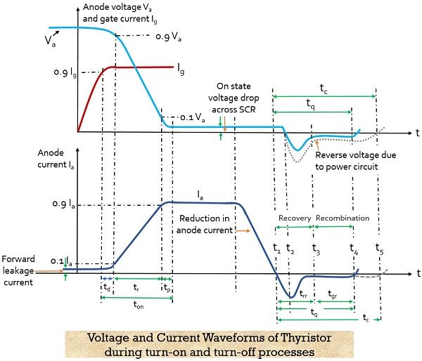
In the above section, we have discussed that a forward-biased thyristor conducts in the presence of positive gate potential at the gate cathode terminal. But you must keep in mind that there exists a transition time within the device between which the device transits from forward off state to forward on state. This time span is generally regarded as thyristor turn-on time and is classified into three intervals i.e., delay time denoted by td, rise time denoted by tr, and spread time, denoted by ts.
Now, let us understand each one separately,
Delay time (td): The delay time of the thyristor depends on the variation in the gate current in forward blocking mode as well as the temperature as it varies the crystal structure of the semiconductor. Delay time is defined as the time instant between the moment when gate current attains 90% of its final value while the anode current attains 10% of its initial value. During delay time, the thyristor remains in the forward blocking mode.
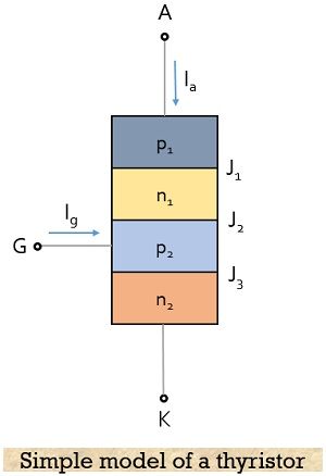
However, internally within the structure of the thyristor, during the delay time, movement of charged carriers takes place. Basically, electrons from the cathode terminal i.e., the n2 layer flow into the p2 region while holes from the p1 layer i.e., anode terminal flows into the n2 layer.
Within the delay time, an anode current flows near the gate terminal in a quiet narrow space. With the increase in gate current and the applied forward anode to cathode voltage, the delay time can be reduced. Generally, its value is in microseconds.
Rise time (tr): Rise time is defined as the time taken by the anode current to rise from 10% of its value to 90% of the same. We have discussed in delay time that it corresponds to the time when anode current reaches 10% of its initial value. Thus, the rise time is started once the delay time gets over.
For the rise time, it is said that the magnitude and rate with which gate current gets build-up is inversely proportional to the rise time. In this time being, a huge amount of charged carriers is present in the gate region and they head towards the cathode to occupy the cross-sectional area of the thyristor. Also, at the same time carriers from the p1 layer are injected into the n1 layer due to the biasing conditions of the junction. This helps to achieve the forward conduction mode in less amount of time.
Once the on-state value of the anode current is achieved then it is said to be the end of rise time. There is a large amount of turn-on losses in the thyristor during rise time, which is the result of the occurrence of high anode voltage and large anode current simultaneously. The occurrence of these losses over a small conducting region results in the formation of local hotspots that may damage the device.
Spread time (ts): Spread time of the thyristor exists between the time when the anode current approaches 100% from its 90% value. More simply, we can say, spread time is the time within which the anode current rises from 90% to 100%. This is called so because, during the spread time, the conduction gets spread over the complete cathode region of the thyristor. Once the spread time is completed, the value of the anode current reaches a steady state.
Thus, it is said that the turn-on time of the thyristor is the summation of delay time, rise time, and spread time. Generally, the rise time is specified by the manufacturers which is in the range between 1 to 4 microseconds. While the overall turn-on time relies on the anode circuit parameters and gate signal waveshapes.
Switching Characteristics during turn-off
Turning the thyristor off means that the state of the thyristor is changed from on to off and it can be able to block forward voltage.
We have discussed that, once the device gets on then even after the removal of the gate signal, current continues to flow through the device due to the fact that the charge carriers in the four layers favors conduction. To turn it off, a reverse potential must be necessarily applied for a specific time interval when anode current attains 0 value.
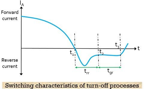
So, the turn-off time of the thyristor is defined as the time being between the instants when anode current becomes 0 and the thyristor attains its forward blocking ability. This turn-off time corresponds to the duration within which all the excess carriers must be removed from the layers of the thyristor. This is nothing but the sweeping out of holes from the outer p region and holes from the outer n region.
The turn of time of the thyristor is categorized into two intervals, namely
- reverse recovery time trr,
- gate recovery time tgr
During the reverse recovery time, the anode current will flow in the reverse direction. Due to this reverse current charged carriers get removed from the pn junction. As the density of the n layer is more than that of the p region, the developed anode voltage leads to a reduction in the reverse recovery time. In the figure shown below, the time interval between t1 and t3 is the reverse recovery time.
Although even when the reverse recovery time is expired, the presence of carriers in the junction J2 will not lead to stop the forward voltage within the thyristor.
This forward voltage can be blocked when recombination of the charged carriers occurs at the junction. The instant where recombination is complete is denoted by t4. However, still, there is the possibility of a supply of forward voltage. This turn-off time generally ranges between 10 to 100 microseconds.
Leave a Reply