Definition: GTO is an abbreviation used for Gate Turn-Off thyristor. It is regarded as a versatile power semiconductor device designed to get turned on and off by the application of gate current.
It was mainly developed to overcome the downsides of the normal thyristor. GTO operates according to its name where the turning off of the device takes place by the action of supply present at the gate terminal.
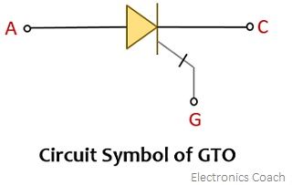
The circuit symbol of gate turn off the thyristor is represented below:
Before having a detailed idea about GTO, let us first briefly understand-
What is a Thyristor?
A thyristor is a 4 layer bipolar current controlled device having 3 terminals. A thyristor is basically designed to conduct a large current when it is on and block high voltage when it is in the off state. This means they can be switched on whenever there will be an appropriate control signal present at the gate terminal of the thyristor.
Now the question arises what is the need for GTO?
Basically, GTO was an invention to overcome the flaws associated with the conventional thyristor model. And due to this reason, there are many similarities between thyristor and GTO. Thyristors has held a great position in the power electronics industry over the past decades. But the major concerning factor of the thyristor is its semi-controllability.
We are aware of the fact that by the application of gate pulse, the thyristor can be turned on however, it does not support the turning off of the device by the action of the gate pulse. As in thyristors, the main supply current must be halted in order to turn it off. However, choppers and inverters fail to reduce the main current to zero value.
Thus, to achieve this, commutation circuits are required in conjunction with the thyristors to properly switch the device off. Thereby providing proper switching characteristics. But the use of commutation circuits has not provided desired switching speed even with fast operating thyristors.
But after the invention of gate turn off thyristors, these disadvantages have been overcome.
Basics of GTO
Gate turn-off thyristor is an advancement of the conventional thyristor. A GTO is designed in a way that it can be turned on by the application of a positive gate pulse at the terminal as well as can be turned off when a negative gate current is applied at its terminal. Now, this is something that was not offered by the conventional thyristor. As the conventional thyristor was made to get on by the action of gate pulse but requires external circuitry for turning off. But GTO gets turned on and off by the action of gate positive and negative pulse respectively.
A GTO is a 4 layer i.e., a p-n-p-n device having 3 terminals which are, anode, cathode, and gate. It is regarded as a two-transistor model which is a combination of PNP and NPN transistors.
A GTO starts conduction when a small positive gate pulse is applied to it but automatically switches to a turn-off state when it is triggered by a negative gate pulse.
Construction of GTO
The figure below represents a pnpn model of GTO with terminals anode, cathode, and gate:
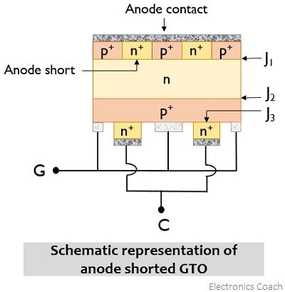
The schematic shown here represents the doping level of the GTO, where the pn and pn layers are doped as p+ np+ n+. Here, to have high efficiency of the cathode, the n+ layer is highly doped. The doping requirement of the p-type gate region is quite contradictory because to have high emitter efficiency this layer should be lightly doped. But to have good turning off characteristics of the GTO, its resistivity should be low thus must be highly doped. Due to this reason, this layer is moderately doped.
The width, as well as the doping concentration of the n-type base region next to the p region, decides the maximal value of forward blocking voltage. In order to have forward blocking voltage in kV, the thickness must be high and it should be lightly doped.
It is clear from the above figure that we have a p+ anode layer over which doping of the n+ layer is done via metallic contact. Such a schematic is known as anode shorted GTO structure. This leads to decreasing of the reverse blocking capacity of the GTO and thus the reverse breakdown voltage of junction J3 gets reduced.
Operation of GTO
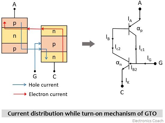
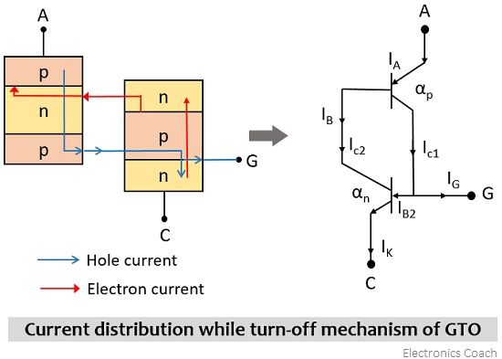
Let us understand the operation of GTO by considering the two transistor analogy shown below:
Turn-on mechanism: There are two ways by which the device can be turned on. Basically, the device gets on when there is a rise in the emitter current as this will automatically increase the current gain α of the transistor. This can be achieved either by rising the anode voltage to cause avalanche multiplication, leading to increase ICBO1 and ICBO2, or by supplying gate current to the circuit.
Generally, the device is turned on by providing current at the p base region through the gate terminal. So, in response to this, the current gains αn and αp start to rise, and once αn + αp = 1, saturation is reached. After attaining the saturation, all the junctions assumed to be in forward-biased condition and GTO gets turned on. After getting on, no supply of gate current is further required to keep the device in conducting state. Thus, an external circuit is required to limit the anode current.
Turn-off mechanism: To turn-off the GTO, a negative gate current must be provided at the gate cathode terminal of the device. Through gate metallization, the holes coming from the anode are collected at the p base region. This causes the drop in voltage of the p base region more than the n emitter region and this reverse biases the junction J3 and terminates further flow of electrons. This happens at the boundary region of the p base and n emitter layers.
At the region of the gate contact anode, current congestion in the form of the high-density filament takes place and this can cause device failure if the current filaments are not handled at the correct time.
Once these filaments disappear completely then no further flow of electrons takes place and the depletion region is generated at the junction J2 and J3. This leads to blocking the forward voltage through the device. This does not turn off the device as at this point of time, the anode to gate current still flows due to diffusion of n base carriers towards the J1. This current is regarded as tail current and undergoes exponential reduction when the excess carriers of the n base region completely recombine.
The decaying of tail current can be achieved at a faster rate when the electron from the n base region gets a different path to reach the anode contact without further emission from the anode.
Advantages
- GTO exhibits fast switching characteristics.
- It is efficient in blocking voltage.
- The absence of a commutation circuit makes it less bulky.
- It is cost-effective.
Disadvantages
- The losses associated are more in GTO as compared to thyristors.
- The gate current used to trigger GTO is quite high.
Applications of GTO
The various applications of GTOs are in high-performance drive systems like in robotics, rolling machines, machine tools, in inverter drives permitting adjustable frequency operation, and in traction purposes. Along with these, it also finds uses in circuit breakers, induction heating, choppers, and several low power applications.
Leave a Reply