Definition: NPN transistor is a current controlled circuit which comprises of three terminal that are emitter, base and collector. It is formed by sandwiching the layer of N-type material between two layers of P-type material. It acts as the current source because it provides current through the base terminal. NPN transistor is exactly opposite of PNP transistor.
NPN transistor can be understood as a Negative-Positive-Negative transistor. This is because the N-type layer of semiconductor consists of electrons as majority carrier. As NPN transistor consists of the emitter of N-type, the majority charge carriers in NPN transistor are electrons.
These electrons when move from low resistance junction, i.e. emitter-base junction to the junction which consists of high resistance region, i.e. collector-base junction, it generates current.
The NPN transistor is preferred over PNP transistor because the mobility of electrons is more than the mobility of holes. In NPN transistors the majority carriers are electrons, and in PNP the majority carriers are holes. Thus, the mobility of charge carriers in NPN will be more than that of PNP.
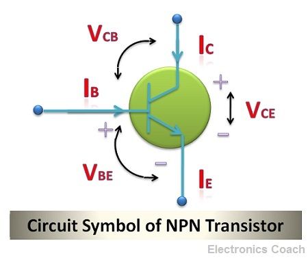
The symbol which is used to denote NPN transistor in electronic circuits is given in the diagram below.
Construction
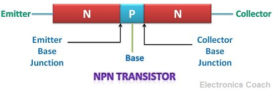
The NPN transistor is formed with the help of three layers of which two are of the N-type semiconductor, and the other one is P-type semiconductor. It is often said that transistor is formed by connecting two diodes back to back. But it is not like that, it is just for imagining the construction.
If it is formed by connecting two diodes back to back, then the resulting structure will have four doped regions because each of the diodes has 2 doped region. In this condition, the base formed by connecting it back to back will not have uniform doping which is the pre-requisite condition for the transistor.
Thus, it is always formed by three layers, in which one is lightly doped, i.e. base, second is heavily doped, i.e. emitter and the last one is collector which is moderately doped. The base of P-type is sandwiched between the emitter and collector of N-type. This results in the formation of an N-type semiconductor.
Are emitter and collector interchangeable?
The emitter and collector region are not interchangeable because the size of the emitter is less as compared to the size of the collector. The collector is made of larger size as compared to emitter because if the size of the collector is large it will collect more and more charge carriers and the heat can also dissipate through the junction of the larger area easily.
Working
The base-emitter junction should be forward biased, and the collector-base junction should be reversed biased. Therefore, the N-terminal of emitter-base junction is connected to the negative terminal of VBE, and the P-terminal of the battery is connected to the positive terminal of the VBE.
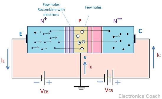
To reverse bias the collector-base junction, the N-terminal is connected to the positive terminal of the VCB and the P-terminal is connected to the negative terminal of the battery VCE. This will make the wide depletion layer at the collector-base junction and narrow depletion layer at emitter-base junction.
When forward biased is applied to the emitter-base junction, the electrons in N-region will repel from the negative terminal of the battery and will move towards the base region. The base region is very small as compared to emitter and collector region. Besides, the doping intensity of base is lowest. Thus, it consists of fewer holes.
Due to few holes in the base region, only a few electrons will recombine with holes. The other electrons which have not recombined yet will move towards collector region. This will constitute current in the circuit. The size of the collector is large so that it can collect more charge carriers and can dissipate heat.
The current in NPN transistor is due to electrons because electrons are the majority charge carriers in NPN transistor.
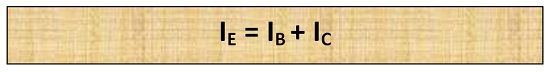
The emitter current in NPN transistor is equal to the sum of base and collector current. Mathematically it can be written as:-
Applications
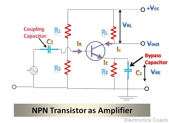
NPN transistor can be used as an amplifier, switch, logarithmic converters, temperature sensors etc.
The transistor is also known as BJT which is an acronym of the Bipolar junction transistor. It is called so because the conduction in BJT is because of bipolar elements, i.e. negative as well as positive. NPN transistor constitutes current because of negative charges particles and PNP transistor constitute current due to holes as majority charge carrier which carry the positive charge.
Leave a Reply