Definition: Unijunction Transistor is a semiconductor switching device having 2 layers and 3 terminals and is abbreviated as UJT. It is called so because of the presence of only one junction. It has the ability to limit large power with a small input signal and is also known as a double base diode.
UJT is a device that possesses negative resistance characteristic that means its emitter current rises regeneratively when triggered. Thus an emitter supply is needed in order to restrict it. In normal operating conditions, it generally absorbs less power and hence is an efficient device.
As it is a low-cost device, hence it is widely used in circuits such as oscillators, triggers and pulse generators etc. It is to be noted that UJT possesses dissimilar switching characteristics from that of the BJT or FET.
Constructional details of Unijunction transistor
The figure below shows the basic structure of a Unijunction transistor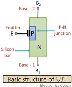
Its structure is almost similar to an N-channel JFET. UJT consists of a lightly doped N-type silicon bar in which a P-type material is diffused thus producing PN junction. Due to the existence of a single PN junction, it is termed as a Unijunction device.
It consists of two ohmic contacts at the end of the bar which is labelled as base 1 (B1) and base 2 (B2). Here, as we can see in the figure above, the structure is not symmetrical as the emitter region is closer to B2 in order to have the optimum electrical characteristic.
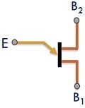
The symbol of UJT is shown below:
Now, let us have a look at the basic arrangement of a UJT:
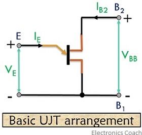
In order to form a complementary UJT, an N-type material is diffused on a P-type bar. A complementary UJT differs from a conventional UJT only by the polarities of current and voltage as the other characteristics of the two are similar.
Working of Unijunction transistor
Let’s now consider an equivalent circuit of UJT shown below:
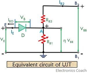
Here, RB1 is variable resistance, due to variation in the resistance with changes in emitter current.
The two resistor of the circuit together constitutes the total resistance which is the resistance between B2 and B1 where the emitter is kept open is known as Interbase resistance RBB.
So, we can write,
RBB = RB1 + RB2
where emitter terminal is kept open.
Normally the value of RB1 is greater than that of RB2.
When a voltage VBB is applied between the two base terminal B1 and B2, the voltage at point A will be,

VA = η VBB
Here, η is termed as an intrinsic standoff ratio and is given by,

and its value is over lastingly less than 1.
Now, let’s discuss the above-stated condition in detail.
Consider a condition when there is no emitter potential supplied to the circuit. In such a case the diode gets reverse biased. Thus, including the barrier potential of the diode, the total reverse biased voltage will become,
VA + VB = ηVBB + VB
As we have considered a silicon bar so in that case the value of VB will be 0.7 V.
If the emitter potential that was previously 0, is increased by a small value and it becomes equal to ηVBB. It will cause the emitter current IE to become 0. This prevents no current to flow through the diode because of equal voltage levels.
On proceeding further, if the emitter potential is increased more, the diode will now get forward biased. This is so because it surpasses the overall reverse biased potential. The emitter potential that puts the diode in forward biased condition is known as peak point voltage and is denoted by Vp.
This allows the emitter current to flow through RB1 to ground, thus ultimately triggering the UJT. The minimum value of IE to trigger the device is known as peak point current of the emitter terminal denoted by Ip.
As the diode gets forward biased and starts conduction, the resistance RB1 decreases quickly. This is so because while conducting, the forward biased diode will inject carriers into RB1 region, thus reducing the resistance as it depends on the doping level.
Due to this reduction in resistance, the drop across RB1 also gets reduced ultimately causing more conduction. This results in greater forward current and the cycle repeats. This emitter current is restricted by the emitter potential of the circuit.
Thus, it is said that UJT possesses negative resistance characteristic as with the increase in emitter current voltage decreases. In order to turn off the device, a negative pulse is then needed.
Characteristics of Unijunction transistor
The figure below shows the characteristic of UJT, it derives the relationship between VE and IE.
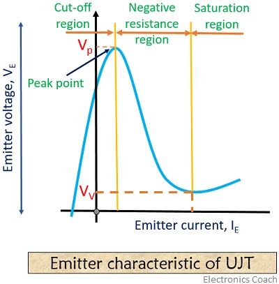
As we can see in the figure, IE does not exceed IEo, which is nothing but equivalent to the leakage current in the reverse direction of BJT. However, it is noteworthy that the above-stated condition is for emitter voltage that lies in the left direction towards the peak point. The region is known as the cut-off region.
As we have already discussed that conduction starts when emitter potential becomes equal to peak voltage. After this emitter potential reduces on, any further increase in IE, that simply shows a reduction in RB1.
This is the reason why the device is said to possess negative resistance characteristic and the region is called negative resistance region.
After this, a valley point is reached, where the device comes to saturation region with any additional increase in the emitter current of the device.
Special features of UJT
- It is a low-cost device.
- UJT is a device with a high pulse current capability.
- It possesses negative resistance characteristic and is a device that absorbs less power during operation.
Applications of UJT
- UJT is a device that is used in thyristor triggering.
- It is used in controlling of DC voltage, in the case of overvoltage detection and measurement of magnetic flux.
- UJTs are used in relaxation oscillator circuitry.
The negative resistance characteristic of a Unijunction transistor is the basis for its operation and due to this, the device can be used as an oscillator.
Leave a Reply