Definition: FET is an acronym used for “field effect transistor”. It is a three terminal unipolar device in which conduction is manipulated with the help of applied electric field. The name itself gives a brief idea about its working principle, “field effect”, these two words clearly indicates it is a transistor controlled by electric field.
Thus, it is also referred as a voltage controlled device in which only majority charge carriers are involved in the conduction mechanism. It comprises of three terminals, i.e. source, gate, and drain.
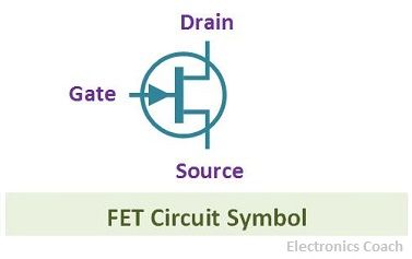
The circuit symbol described in the below diagram clearly illustrates the three terminals of field effect transistor.

History of Field Effect Transistor
In the year 1926, the idea of field effect transistor (FET) was introduced by Lilienfield. After this in the year 1935, Heil had also put light on field effect transistor. But by this time FETs were not much popular. It was in the year 1940, the significance of FETs gain momentum. This is because during the 1940s the research was going on semiconductors at Bell laboratories.
Significance of FET
Before discussing the significance of FET, I would like to share the crucial concept regarding FET. The transistor in its name is often confused with a bipolar transistor. But there exists a vast difference between FET and BJT, i.e. bipolar transistor.
Although both are transistors and both, involve conduction of current and also both have three terminals, but the similarities end here. The BJT uses injection and collection of minority charge carriers, and this process of injection and collection is done during forward biasing of the P-N junction. On the contrary, the FETs uses an electric field to vary the depletion width during reverse biasing of the junction.
Thus, the conduction in BJTs involve majority carriers as well as minority carriers, but the conduction mechanism in FETs is only due to majority charge carriers. This is the reason FETs are termed as a unipolar device.
Water Analogy to understand the concept of FET
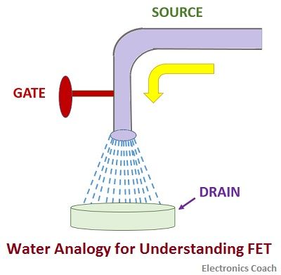
To understand how an FET works, let’s use an analogy. Analogies often make things simple to understand even a complex concept. The water source can be understood as the source of FET, the vessel which collects water is analogous to the drain terminal of FET. Let’s have a quick look at the below diagram, after that understanding the concept of FET will be a cake walk.

Now, can you guess what gate terminal is analogous to? If you are thinking of water tap then yes, you are correct. It is nothing other than the controlling tap which controls the flow of water. Now, the way in which the controlling tap modulate the quantity of water coming from the outlet, in the same way, the voltage at gate terminal controls the flow of current from source to drain terminal.
Construction and Working of FET
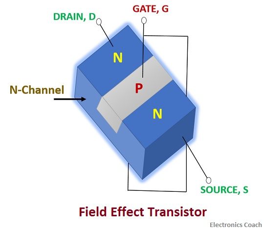
The semiconductor is the basis of all FETs. Depending on the channel we are using, i.e. N-channel or P-channel, the semiconductor specimen will be used. If we are designing N-channel JFETs, then the channel will be of an N-type semiconductor. And in the middle of the opposite phases of the specimen will be diffused with the P-type semiconductor.

The P-type semiconductor bar will act as a gate terminal. The opposite ends of the P-type semiconductor will be connected together to form a common gate terminal. Thus, there will be two P-N junctions on either side of the gate, and that will be termed as source and drain terminal.
Components of FETs
- Channel: This is the area in which majority charge carriers flow. When the majority charge carriers are entered in FET, then with the help of this channel only they flow from source to drain.
- Source: Source is the terminal through which the majority charge carriers are introduced in the FET.
- Drain: Drain is the collecting terminal in which the majority charge carriers enter and thus contribute in the conduction procedure.
- Gate: Gate terminal is formed by diffusion of a type of semiconductor with another type of semiconductor. It basically creates high impurity region which controls the flow of carrier from source to drain.
Classification of FETs
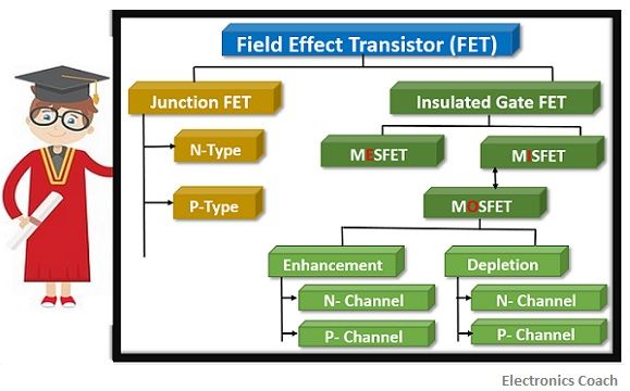
The classification of FET can be understood with the help of chart described in the below image. The FETs are mainly described in two types that are JFET (Junction field effect transistor) and Insulated Gate field effect transistor.

Junction Field Effect Transistor: The junction FET is nothing but the FET in which conduction is established by variation of depletion width when the junction is reversed biased. It comprises of two types according to the construction that is N-Channel and P-Channel.
Insulated Gate Field Effect Transistor: The insulated gate FET is one in which gate is insulated by an insulation material from the semiconductor specimen. These are of two types MESFET (Metal Semiconductor Field Effect Transistor) and MISFET (Metal-Insulator-Semiconductor Field Effect Transistor).
Both MESFET and MISFET uses metal-semiconductor junction rather than conventional P-N junction. But the feature that distinguishes both is the use of insulation material in case of MISFET while there is no insulation material in MESFET.
MOSFET is the subtype of MISFET in which oxide layer plays a crucial role in providing insulation between the gate and other terminals. MOSFETs work in two modes that are Depletion mode and Enhancement Mode. In depletion mode, there exists a physical channel while it is not so in Enhancement mode.
The depletion and enhancement MOSFET can again be designed in two ways by using N-channel or P-channel. This was the brief description about FETs.
Leave a Reply