Definition: Op-Amp is an abbreviation for the operational amplifier is basically a three terminal voltage amplifying device. It is a high gain, negative feedback amplifier that provides stabilized voltage gain.
Op-amps are considered as the basic building blocks of the circuits in the field of analogue electronics. These are designed in such a way to be used with external feedback components such as resistors, capacitors in between input and output terminals.
This 3 terminal device consists of two high impedance input ports alongwith an output port.
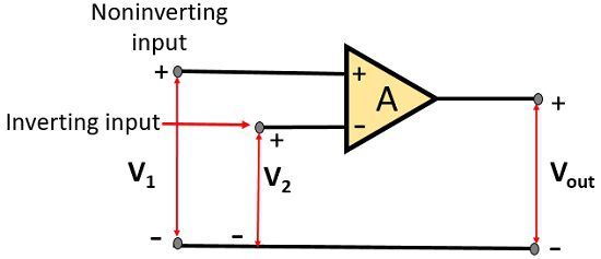
The two input terminal has one inverting input with a negative sign and one non-inverting input with a positive sign.
As op-amps have high input impedance and low output impedance moreover has the ability to amplify signals of the frequency range from 0 Hz to 1 MHz. It can be used to amplify ac as well as dc input signals.
Op-amps were basically designed to perform mathematical operations like addition, subtraction, multiplication, differentiation, integration etc.
But, today op-amp provides a variety of other uses such as phase shifting, scale changing, sign changing, in oscillator circuits, pulse generators, comparator, converters etc.
An op-amp act as a versatile device and can perform countless tasks when manufactured with integrated transistors, diodes, resistor and capacitor. Op-amps provides extremely high voltage gain, typically of order 200,000.
The output of an op-amp is a difference value of the two inputs applied. So, we can say the amplifier is a differential amplifier that provides an amplified version of the differential input signal.
History of an Op-amp
Op-amp was firstly built with a vacuum tube but in the early 1960s, transistors replaced vacuum tubes. When IC technology arrived, it became possible to place the Op-amp into a single 8 lead package.
The figure below shows the pin diagram of an Op-amp-
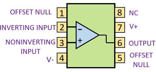
Fairchild in 1965 introduced the 1st generation 709 and in 1968, still popular 2nd generation 741 Op-amps introduced. An Op-amp IC 741 has become an industry standard.
Schematic symbol of an Op-amp
The diagram shown below shows the schematic symbol of an Op-amp-
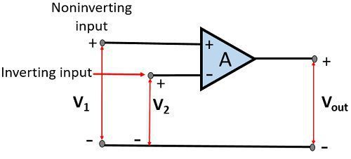
Here, A represents voltage gain
V1 is the input at non-inverting terminal and
V2 is the input at inverting terminal of the Op-amp.
So, we will have a differential value at the input
V1 – V2 = Vin
And at the output, we have an amplified output with gain
Vout = A Vin = A (V1 – V2)
As we have already discussed that positive indicates the non-inverting terminal and negative indicates the inverting terminal.
The input at the positive terminal will get amplified at the output in the same way it is. But, the input at the negative terminal will give us an inverted amplified output.
From the above discussion don’t get confused about the thing that plus voltage means V1 is positive and minus means V2 is negative as it is not so. It also does not mean that positive voltage is to be applied to the positive terminal and the negative voltage is to be applied to the negative terminal.
The voltage at the output will be directly proportional to the difference of two input signals.
Op-amp can be operated in a single or double ended mode that totally depends on whether the input is applied to only one of the terminals or both. The most commonly used configuration is 2 input and 1 output.
Equivalent circuit of Op-amp
The figure shown below will help you to analyse the basic operating principle of an Op-amp
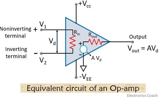
The output voltage is given by
Vout = AVd = A (V1 – V2)
Here, AVd is equivalent Thevenin’s voltage source and Rout is Thevenin’s equivalent resistance.
The above equation indicates that Vout is proportional to the algebraic difference of two input voltages i.e., we can say basically the difference is amplified and not the original input.
Voltage Transfer Curve
This curve is drawn between the output voltage Vout and difference input voltage Vd where gain A is kept constant.
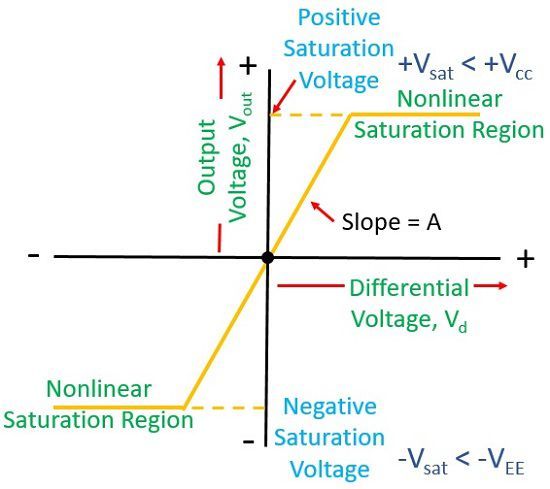
The above curve is known as the Ideal voltage transfer curve.
It is called so because while drawing the above curve we have already assumed the output offset voltage to be 0.
When we talk about normal Op-amp, the output offset voltage is nearly 0 and we ignore it for simplification purpose in the calculation. It is to be noted here that the curve is not drawn to scale; as we will have a vertical line in such case as the voltage gain is very large. In the above figure, we have seen that output voltage Vout cannot exceed positive and negative saturation voltage.
Simply put, the output voltage Vout increases in direct proportion to the differential input voltage Vd until it attains saturation value, after which it becomes constant.
Basic Op-amp Circuit
The basic circuit of an Op-amp is shown below: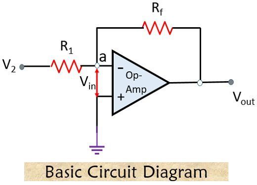
As we can see, an input signal V2 is applied through resistance R1 to the inverting terminal of the Op-amp. The output voltage is then fed back to the same input terminal through resistance Rf. The non-inverting terminal of Op-amp is connected to earth.
Now, let us have a look at the equivalent circuit of the basic circuit of op-amp:
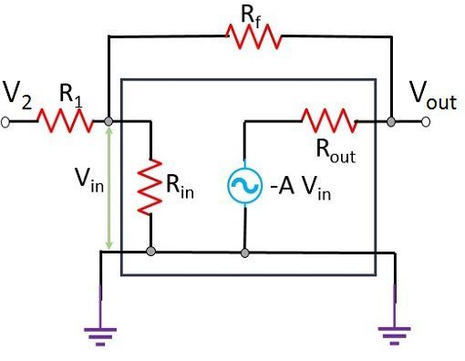
Here, the equivalent circuit of op-amp consists of input resistance Rin and output voltage source and resistance. An ideal op-amp offers infinite input resistance with 0 output resistance and infinite voltage gain.
Let’s redraw the above circuit so as to have a better idea of the whole concept.
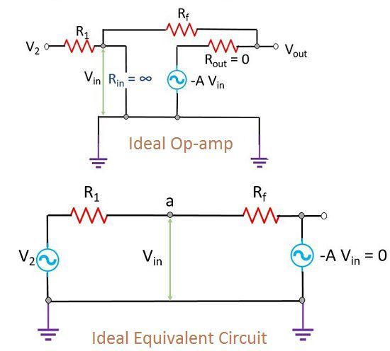
Using superposition theorem Vin can be solved in terms of components due to each source-
Let us assume that here -A Vin to be 0 and the only source is V2

Now, when we assume V2 to be 0, for source –A Vin only

Therefore, the total input voltage we will have
![]()

Or 
For the condition A >> 1 and A R1 >> Rf usually true,


The above equation shows that the ratio of overall output to input voltage depends only on the value of resistors R1 and Rf provided A is very large.
Thus we can say by using absolute resistor values of R1 and Rf, we can have a wide range of gain. The gain will be almost accurate as that of resistors used and is affected only slightly by temperature and other circuit factors.
Virtual Ground Concept
As we are already aware of the fact Vout is to be limited to supply voltage
So, 
= 100 or 150 µV
The value of Vin as compared to the other voltages is very small and can be considered to be 0 V.
As Vin is almost 0, but not exactly 0 as Vout depends on Vin. This Vin ≈ 0 leads to the concept of virtual ground.
Virtual ground implies that though input voltage is nearly 0 there is no current through amplifier input to the ground. Let us see the figure below to have a clear concept of virtual ground.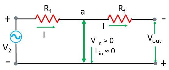
With Vin ≈ 0, a short is considered to exist. But here the concept is virtual short, due to which no any current passes through the short to the ground. So, the current through R1 and Rf will flow.
The current equation for above circuit is given as-![]()
Or 
Although the above figure is not physically correct, it allows an easy means for determining the overall voltage gain.
The overall idea of virtual ground comes into focus when Vin ≈ 0.
Now the question arises, How Vin can be approximately 0?
On application of V2, point ‘a’ gains some positive potential but at the same time as Vout comes into existence. Due to this, some part of Vout is fed back to point ‘a’ in phase opposition of already existing voltage V2 because of negative feedback. Thus causing algebraic sum to be almost 0.
For an Op-amp differential and common mode, signals are very popular terms.
Differential input signals as the name suggests is the value obtained due to the difference in two input signals.
Vd = V1 – V2
But common mode input signal is the average of the two input signals.
Vcm = (V1 + V2) /2
Characteristics of an Op-amp
While designing Op-amp circuits or in troubleshooting both ac and dc characteristics are to be considered as Op-amp is a dc amplifier.
DC Characteristics
When we talk about an ideal Op-amp, it does not draw any current from the source driving it and the circuit response does vary with temperature variation. But, an actual Op-amp operates in a different way i.e., Op-amp input draws current from the source and the two input responds differently with that voltage and current.
These non-ideal characteristics are discussed below:
- Input Offset Voltage: Input offset voltage Vin(offset) is the voltage which is applied to the input terminals to balance the amplifier. When the inputs of the op-amps are grounded, there exists an output offset voltage.
- Input Bias Current: For proper operation of an operational amplifier, a dc bias current is needed to be supplied at the input of the differential amplifier. This current is of the order of pA to nA. It is given by the average of dc bias current at both the inputs of the differential amplifier.
- Input Offset Current: As Op-amp is formed by the combination of two input transistors that are not accurately matched. This mismatching requires a different bias current at the input of each transistor. This difference between the two bias currents is termed as input offset current.
Difference amplifier has excellent ability to cancel out or reject certain types of unnecessary voltage signals. Noise can be that undesired signal. These noise signals are not meant to be amplified in the amplifier.
As noise signals appear equally at both inputs of the circuit. It means that undesired signal appearing at both the inputs will be rejected by the differential amplifier. A measure of rejection of the signal that is common to both the input is known as common mode rejection.
CMMR is given as the ratio of different voltage gain to common mode voltage gain.
 AC Characteristics
In industrial circuits, Op-amps are used strictly as dc amplifiers but they have ac applications also.
- Slew Rate: It represents the maximum rate by which the output voltage changes when a large input signal drives the amplifier. Slew rate is basically the rate of change of output voltage rapidly but not instantly when a differential input is applied at the input of Op-amp. The slew rate of a typical Op-amp 5,00,000 V/s or 0.5/µV.
- Full Power Response: When a large amplitude sinusoidal signal is applied, the maximum frequency amplified by the Op-amp without distortion is known as full power response.
- AC Noise: The undesirable signals at the output of an Op-amp are termed as noise. AC noise is categorised as mainly internal and external noise. External noise is caused by external effects or interference but internal noise is caused by the internal circuitry of the amplifier.
Applications of Op-amp
Op-amp finds its application in a wide variety of fields. These are used in the construction of active filters that can provide the high pass, low pass, bandpass or band-reject functioning.
They can be used as comparators or in the construction of oscillators.
Leave a Reply