Definition: PIN diode is formed by sandwiching intrinsic layer (high resistivity about 0.1 Ω-m) between P-type and N-type semiconductor to create an electric field between them. Due to this large magnitude of the electric field, the electron-hole pair generation will augment up to a large extent and this, in turn, can process even a weak input signal.
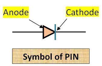
The width of these depletion layers is large due to which capacitance will decrease because capacitance decreases with the separation between electrodes. Here P-type and N-type region are acting as anode and cathode respectively.
The symbolic representation of the PIN diode is shown below:

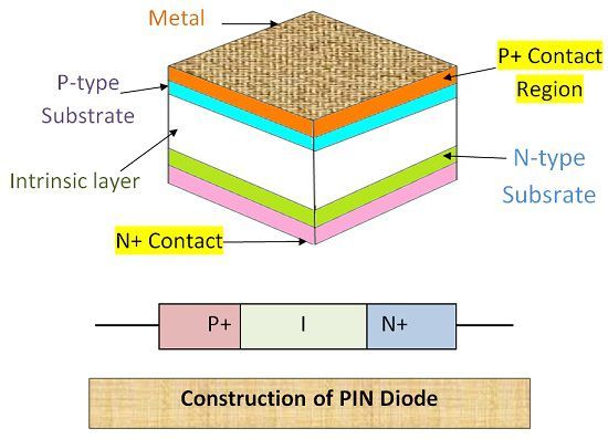
Construction of PIN Diode
Pin diode consists of two layers of semiconductors and one layer of intrinsic material in between them. The Semiconductor layer are usually of P-type and n-type. Pin diode can be constructed in two ways using planar structure and mesa structure. In a planar structure, a very thin epitaxial layer is fabricated on the P-type substrate. This epitaxial layer consists of P+ regions.

Similarly, an epitaxial layer is fabricated on N-type substrate, and that will be comprised of N+ region. And in between these semiconductors, a layer of intrinsic material of width 10-200 microns and resistivity 0.1 Ω-m is introduced. Semiconductor layer provides ohmic contacts.
Working of PIN Diode
When PIN diode is unbiased, the charge carriers will flow from N-type region to intrinsic region due to the concentration gradient. Thus, the width of the depletion region at NI junction (Intrinsic and N-type material) will be more on N side and less on I-side.
The reason behind this is N-type material is heavily doped while the Intrinsic layer is not doped or doping level is extremely low. Thus, when charge carriers (electrons-majority carriers in N-type) flow from N-type to Intrinsic layer the depletion region will be created, but the width of it on both the sides of N-I junction will be different.
Swept-Out Voltage
When the PIN diode is reversed biased, then the reverse voltage will keep on increasing the width of the depletion region at N-I junction. Because reverse biasing increases the width of the depletion region.
It will increase up to an extent when the entire intrinsic layer is swept or free from charge carriers. The value of the reverse voltage at which the whole intrinsic layer is swept of charge carriers is called Swept-out voltage. The value is -2V.
Impact of Reverse Biasing
The Pin diode in reverse biased is used in various devices working at microwave frequencies such as microwave switch. Thus, if all the charge carriers are not removed from the intrinsic layer, it may lead to the flow of current. And for switching purpose, even a small amount of current flow can make the device useless.
Impact of Forward biasing
When the PIN diode is forward biased the gradual increase in forward voltage decreases the width of the depletion layer at P-I junction (P-type and Intrinsic layer junction).
Thus, with the reduction in the width of depletion layer current starts increasing. In forward biasing it acts as a variable resistor by providing variable resistance and in reverse biased it provides infinite resistance and thus acts as a perfect switch.
Thus, with the decrease in the width of depletion layer current starts increasing. Thus, in forward biasing it acts as a variable resistor by providing variable resistance and in reverse biased it provides infinite resistance and thus acts as a perfect switch.
Characteristics of PIN Diode
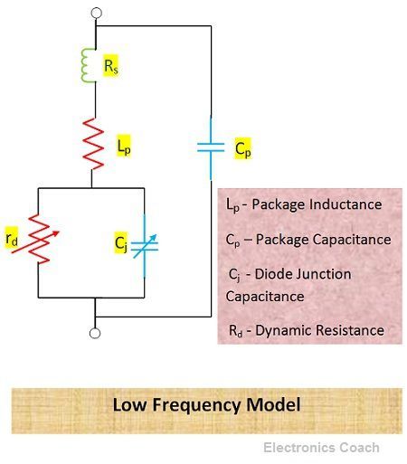
At lower frequencies, the charge carriers from intrinsic layer can be detached easily as we have sufficient time. Low frequency means time factor is large as the frequency is inversely proportional to time.

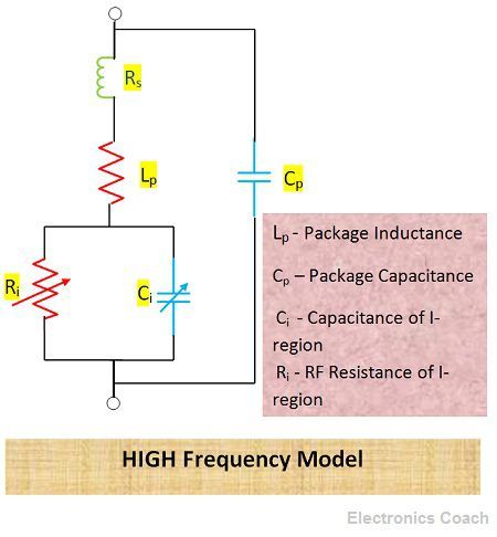
But at the higher frequency, the time factor is low; thus, the charge carriers cannot be removed completely. Therefore, at the higher frequency, it behaves as the resistor having range between 0.1kΩ to 10kΩ.

Applications of PIN Diode
- As High Voltage Rectifier: PIN diode is used as high voltage rectifier. The large width of intrinsic layer imparts the ability to the diode to tolerate high reverse voltage without leading to the breakdown of the diode. Thus, rectification at high voltage can be implemented with PIN diode.
- As Radio-frequency Switch: PIN diode can be used as RF and microwave switch, but in this case, the diode needs to be operated in reverse biased region. The width of intrinsic layer is comparatively more than layers of semiconductor, thus, more the width more will be the separation between the semiconductor layer and the less will be the capacitance.
Thus, if a diode is to be operated as a switch, the capacitance should be negligible. It should not store any charge and immediately changes from conduction to insulation and vice versa.
- As Photodiode: PIN diode can also be used as a photodiode. The conversion of electric current into the light is performed in the intrinsic region of the diode. Thus, the more the width of the intrinsic region more will be the efficiency of the diode for generating light.
- As Attenuator and RF protection Circuit: When PIN diode is forward biased, it works as a variable resistor. Thus, it can be used for protection of RF circuit from high current which may damage the circuit. When the forward biased is increased the resistance decreases suddenly, thus, it can be used as an attenuator.
Advantages of PIN Diode
- High reverse breakdown voltage: The width of the depletion layer in PIN diode is large. It imparts it the ability of high reverse breakdown voltage. Thus, it is suitable for protection of circuits from a large current.
- High Capacitance: The width of intrinsic layer is large due to which capacitance of diode is low. As the capacitance of a device is inversely proportional to the distance between the electrodes.
- Photodetection: Due to the large width of the intrinsic layer, the photons striking the surface will be more. And the generation of the electron-hole pair will also increase. Due to which more current will flow. Thus, PIN diode helps to achieve improved photodetection.
Disadvantages of PIN Diode
High Reverse Recovery Time: The PIN diode has high reverse recovery time due to which power losses are significant.
Raj Kumar maurya says
Thanks sir for all topic. Please provide notes about power electronics. Like- SCR , DIAC , TRIAC, UJT, INVERTER , CONTROLLED RECTIFIER etc.