Definition: Tunnel diode is a heavily doped diode which possesses high conductivity due to the higher concentration of impurity atoms. It is different from a conventional P-N junction in terms of doping density.
Its principle of operation is tunneling.
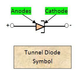
The schematic symbol of Tunnel Diode is represented in the below diagram.

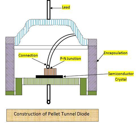
Construction of Tunnel Diode
A tunnel diode is usually constructed with Gallium. The compounds of Gallium such as Gallium Arsenide and Gallium Antimonide are considered appropriate for tunnel diode. The reason behind this is the ratio of the peak value of forward current and the value of valley current. The value of this ratio is high in case of Gallium which is desirable.

In the case of Gallium, this ratio is approximately equivalent to 20 whereas in the case of Germanium it is comparatively low i.e. 10. But in the case of silicon it is extremely small (about 3). Thus, Silicon is not preferred for the construction of Tunnel Diode.
Germanium, Gallium Arsenide or Gallium Antimonide is used for the fabrication of Tunnel Diode. It was invented by Dr Leo Esaki. Thus, it is also called Esaki Diode.
Working Principle of Tunnel Diode
It is similar to typical P-N junction diode, but its high doping density changes its conductivity up to a large extent. In normal P-N junction diode, the doping concentration is 1 atom in108 atoms. But in the case of Tunnel Diode, it is 1 atom in 103 atoms. Due to the higher concentration of impurity ions, the width of the depletion layer decreases, and it becomes about 10-5mm.
Tunneling
The charge carriers can easily cross the junction as the width of the depletion layer has reduced up to a large extent. Thus, charge carriers do not need any kinetic energy to move across the junction; they simply punch through the junction. This effect is called Tunneling. Thus, it is called Tunnel diode.
Due to Tunneling, a large value of forward current is generated even when the value of forward voltage is low (approximately 100mV). It can operate in forward biased as well as in reverse biased. You must be thinking, How in reverse biased? But yes, due to high doping it can operate in reverse biased too. But it is usually operated in forward-biased only.
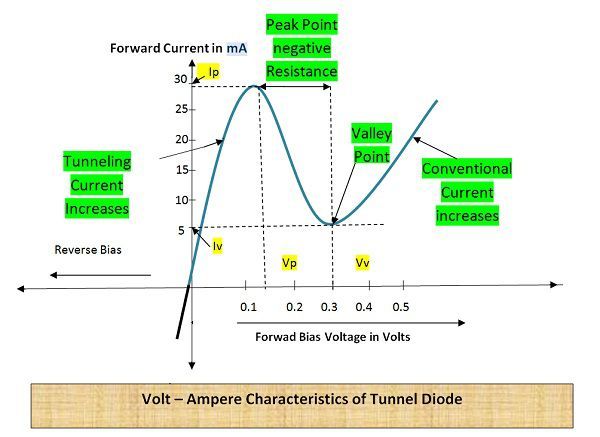
The reverse breakdown voltage also gets reduced due to the reduction in barrier potential. It becomes approximately zero due to which even a small reverse voltage can lead to the breakdown of the diode. As a consequence of this, the negative resistance region is created. You can understand this with the help of volt-ampere characteristics of the tunnel diode.
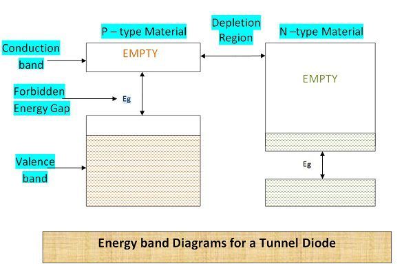
Explanation of Tunneling with the help of Energy band Diagram
When the P-type semiconductor is heavily doped, then the concentration of holes is higher. On the contrary, the concentration of electrons is lower. While in heavily doped N-type semiconductor, the concentration of electrons is higher. On observing the energy band diagram in this scenario, it can be said that electrons fill the lower energy levels of the conduction band in N-type region.

On the P-side the conduction band is entirely empty. The filled band in N-type is exactly opposite to filled side valence band on P-type. Thus, in this case, no tunneling can take place. Tunneling will be there if filled band on one side is opposite to empty band on another side.
Effect of Biasing on Energy band Diagram
If reverse biased is applied P-region will move up, thus energy level of P-region will attain the higher level. In this case, the filled valence band of P-region is exactly opposite to empty conduction band of N-region. Therefore, current will flow in reverse biased too because of movement of charge carriers. And this current will increase with the increase of reverse voltage.
When forward-biased is applied to it, the N-region will move up and occupy higher energy level. And the maximum tunneling occurs when the lower filled conduction band of N-type is exactly opposite to empty conduction band of P-type. With the increase in forward voltage more and more tunneling will occur. And the forward current will increase and attains peak value of forward Current (Ip) at the peak value of forward voltage (Vp), i.e., 100mV.
When the forward voltage is increased further then the N-type region further move upward. And at a particular time, the stage is reached when no more tunneling takes place because entire electrons in the conduction band of N-type material has moved to the P-type region. And the empty energy levels from both P-type and N-type is opposite to each other.
Note: Here P-region or N-region moving upwards means they are occupying higher energy levels. This is so because when they are biased, forward or reverse external battery source supply energy.
Volt-Ampere Characteristics
The volt-ampere characteristics of Tunnel diode is different from the conventional P-N junction. This is due to negative resistance section in the case of the tunnel diode. When forward Biased is applied the current starts flowing and attains peak value, Ip. But when voltage cross peak value of forward voltage Vp(100mV), current starts decreasing. This is negative resistance region.

The current reaches minimum value i.e., Valley current Iv at Valley voltage Vv.
Advantages of Tunnel Diode
- It is a low-cost device.
- Tunnel Diode is immune to noise interference.
- It is simple, and it has high speed of operation.
Disadvantages of Tunnel Diode
- It do not provide isolation between input terminals of diode and output terminals of diode.
- It is a low power device. Thus, it is more prone to be damaged by heat and electricity.
Applications of Tunnel Diode
It is used as a switch, oscillator, amplifier etc. It can be used as a high-frequency component because of its fast response, but due to the availability of better devices, it is not preferred.
Leave a Reply