Definition: Schottky diode is a metal-semiconductor junction which does not store charge carriers at the junction because it has no depletion layer. It finds its application where fast switching is needed.
Significance of Schottky diode: When a P-N junction diode is forward biased, it starts conducting, but when it is reverse biased, it stops conduction. But this transition from conduction to insulation is not instant. Diode takes some time to reach a steady state of no conduction when it is reverse biased.
This happens because during forward biasing charge carriers move across the junction and when it is suddenly reverse biased, some of the charge carriers are still at the junction, but they have not recombined yet.
Thus, this phenomenon is called charge storage. Due to this charge storage diode takes time while switching. The time taken by the diode to achieve a steady state of no conduction in reverse biasing is called reverse recovery time. The effect of reverse recovery time is negligible at frequencies below 10MHz, but at high frequencies this effect is significant.
To eliminate this problem Schottky diode was constructed. How this Schottky diode overcome this problem. You can understand that with the help of its construction and working.
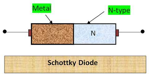
Construction of Schottky Diode
It is formed of metal and semiconductor. The metal such as gold, silver, molybdenum, tungsten or platinum is used. And N-type semiconductor is used. Usually, Gallium is used as a semiconductor for the schottky diode. Although Silicon can be used for low frequencies operation.
Different materials used in construction results in different characteristics of resulting Schottky diode.
Working of Schottky Diode
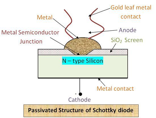
Metals have electrons as majority carrier, and N-type semiconductor also possesses electrons as majority charge carrier. Thus, when a metal-semiconductor junction is unbiased, then current doesn’t flow in a diode. This is because electrons in N-type region do not possess sufficient energy to transit from N-type junction to metal. But when the junction is forward biased then electrons acquire energy to cross the barrier.
Hot Carrier Diode
This barrier is called Schottky Barrier. The electrons which are moving from N-type to metals are termed as hot carriers. They are called so because when the junction is forward biased electrons acquire a significant amount of energy. And they enter metal junction with this high magnitude of energy. That’s why diode is also called hot-carrier diode.
The best thing about Schottky diode is its fast switching ability. There is no role of the depletion layer in the case of Schottky diode, that’s the reason it possesses fast switching than P-N Junction diode. Metals and N-type semiconductor have electrons as majority charge carriers.
Thus, the entire current is due to bulk carriers. There are no holes, so there is no depletion layer. Thus, there is no charge storage at the junction.
Due to the absence of charge storage, the Schottky diode can be easily switched from forward biased to reverse biased. A p-n junction is bipolar because it consists of both electrons as well as holes as majority carriers, but Schottky diode is unipolar because it involves only one charge carrier i.e. electron.
The barrier potential of Schottky diode lies in the range of 0.2-0.25V which is much lower than the barrier potential of Silicon 0.7 V. The reason behind this low barrier potential is, again the absence of depletion layer.
Thus, no significant current flows from metal to semiconductor when the diode is reverse biased. Thus, the current flows only in the case of forward biased of the metal-semiconductor junction.
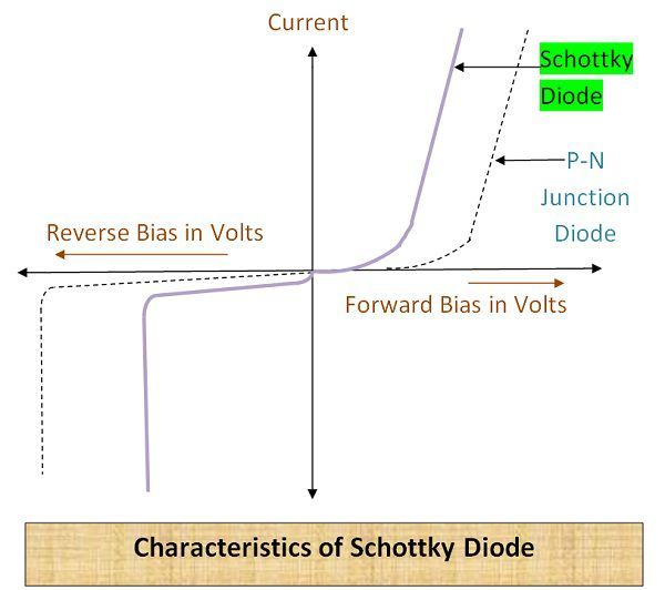
Volt –Ampere Characteristics of Schottky Diode
It can be seen from its V-I characteristics that current starts increasing at very low forward voltage. While in the case of P-N junction this current starts increasing after providing sufficiently high forward voltage. Similarly, the reverse voltage at which current starts increasing is also low in case of Schottky diode. Thus, its reverse breakdown voltage is also low.
Advantages of Schottky diode
- It possesses high switching speed.
- Due to high switching speed, its reverse recovery time is very less as compared to other bipolar diodes.
- The value of forward voltage in the case of this diode is also minimal comparatively other bipolar diodes.
Disadvantages of Schottky Diode
- It possesses a significant value of leakage current.
- The reverse breakdown voltage of these diodes is very small. Thus, even a small amount of reverse voltage can damage it.
Applications of Schottky Diode
- It is used as Schottky TTL in digital devices as these devices need fast switching.
- A Schottky diode is the most significant component for digital computers, as the performance of digital computers is determined by switching speed of diodes.
These are the advantages, disadvantages and applications of the Schottky diode. Due to its fast switching it is used in TTL circuits.
akanksha nema says
Perfectly explained…helped me in clearing my many doubts..
Thanku..
Krati P says
Thank you for your support !!! It’s a matter of huge pleasure for us that our contents are helping you to explore concepts of electronics.
Next Tube says
best explaination ever