The voltage doubler is a device which delivers double the peak voltage (maximum voltage). It comprises of capacitor filter circuit which delivers double DC voltage of the peak input AC voltage. Voltage doublers are of significant importance in devices which needs high voltage and low current. Some of the devices which fall in this category are cathode ray oscilloscopes, picture tube used in TV receivers and in the display of a computer.
Half – Wave Voltage Doubler
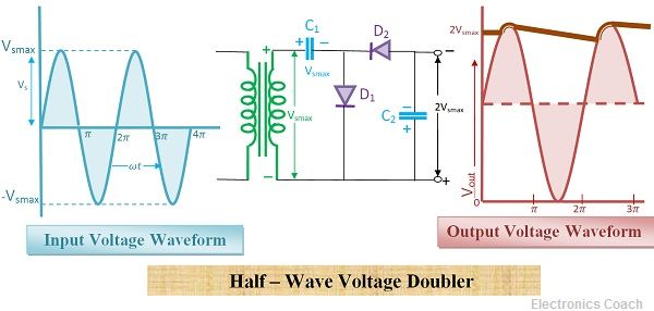
The half wave voltage doubler consists of two diodes D1 and D2 and two capacitors C1 and C2. When the positive cycle of AC approaches the circuit the top of the secondary winding of the transformer is positive while the bottom of the secondary winding is negative. This makes the diode D1 to operate in forward biased mode.
When the diode D1 is forward biased, it behaves as a short circuit, and thus capacitor C1 starts charging. Let the AC voltage be Vsmax then the capacitor C1 also gets charged to its peak value, i.e. Vsmax. The polarity of the voltage across capacitor C1 is shown in the diagram below.

During positive half of AC cycle, the diode D2 is reverse biased thus the diode D2 becomes an open circuit, and the capacitor C2 will remain uncharged.
This happens because when the top of a secondary winding of a transformer is positive, the P-terminal of diode D1 is positive while N-terminal is negative this makes the diode forward biased. On the contrary, the N-terminal of diode D2 is positive, and its P-terminal is negative which makes the diode D2 reversed biased.
During the negative half cycle of AC signal, the diode D1 will be reversed biased because in this case top of the secondary winding of the transformer is negative and bottom of the secondary winding of the transformer is positive.
Therefore, the diode D2 will be forward biased. Thus, the capacitor C1 will not get charged during negative half cycle while the capacitor C2 will gets charged to its peak value.
In order to determine the voltage across capacitor C2, let’s apply Kirchhoff’s law to the circuit starting from the secondary winding transformer’s bottom point and moving in clockwise direction.
-Vsmax – Vc1 – Vc2 = 0
Or Vc2 = Vsmax + VC1
= Vsmax + Vsmax
= 2Vsmax
Now, the capacitor C1 gets charged to Vsmax and capacitor C2 gets charged to 2Vsmax. During the negative half of AC signal when the diode D2 is reversed biased the capacitor gets discharges through the load. And thus, the output voltage thus produced is 2Vsmax. Thus, the output voltage thus produced is double of the input AC voltage, this is the reason it is called voltage doubler.
Full – Wave Voltage Doubler
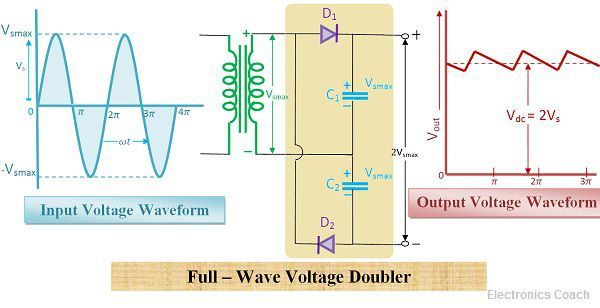
In full wave rectifier when the positive cycle of AC signal is applied to the secondary winding of the transformer, the diode D1 gets forward biased, and capacitor C1 starts charging. The capacitor C1 gets charged to its peak voltage, i.e. Vsmax. And the diode D2 will be reversed biased during the first half of AC signal. And thus, diode D2 will be an open circuit, so capacitor C2 will not charge during this phase of AC input.

When the negative half cycle of AC is applied to the full wave voltage doubler circuit, the diode D2 will be forward biased. Due to this, the capacitor C2 starts charging. It will charge to its peak value, and the polarity will be same as the represented in the diagram.
Now, both the capacitors C1 and C2 are charged to its peak value Vsmax. When the load is connected to the output terminal, the capacitor will get discharged through the load. Thus, the total voltage will be given as: –
Total Voltage = Voltage across C1 (Vc1) + Voltage across C2 (Vc2)
Voltage across load (VL) = Vsmax + Vsmax
VL = 2Vsmax
Thus, the voltage produced finally at the output is double of the input voltage. Thus, it is called Full wave voltage doubler.
Advantage of Full Wave Voltage Doubler over Half Wave Voltage Doubler
The ripple frequency of the output signal obtained by full wave voltage doubler is twice of the ripple frequency of the output signal obtained by half wave voltage doubler circuit. Thus, these higher ripple frequencies can be easily filtered in comparison to low frequencies ripples.
Disadvantage of Full Wave Voltage Doubler over Half Wave Voltage Doubler
The only drawback of full wave voltage doubler is that it does not provide common point between input lines and output lines for earthing. While in case of half wave voltage doubler there is a common point between input and output lines. Thus, earthing of the circuit is possible and easier in case of half wave voltage doubler circuit.
In the table given below, the comparison between half -wave voltage doubler and full wave voltage doubler is provided. Although both circuits provide double of the supply voltage, each of this two circuit has some advantages and disadvantages. Thus, it should be used in application keeping in mind its pros and cons.
Comparison Between Half - Wave and Full - Wave Voltage Doublers
| Parameters | Half - Wave Voltage Doubler | Full - Wave Voltage Doubler |
|---|---|---|
| Ripple Frequency | Input signal's frequency (f) | Twice of input signal frequency (2f) |
| Ripple Content | High | Low |
| Voltage Regulation | Poor | Better than half - wave voltage doubler |
| Common point between input and output lines for earthing | Available | Not Available |
| Maximum Voltage across each capacitor | 2Vsmax | Vsmax |
| PIV Rating | 2Vsmax | 2Vsmax |
Besides, we can even get triple and quadruple of the input voltage. This can be done by modifying the doubler circuit by adding diodes and capacitor.
Leave a Reply