Definition: Voltage regulator is a device that maintains a constant dc output voltage irrespective of the changes in input voltage or load conditions. The ac ripple voltage that is not removed by the filters is also rejected by the voltage regulators.
The combinations of elements present in the design of voltage regulator ensure to have a constant output voltage with a variable input supply.
Whenever there is a need to have a steady and reliable output voltage then voltage regulators are the most preferred circuits.
Voltage regulators also display protective functions such as overvoltage protection, short circuit protection, thermal shutdown, current limiting etc. It can be a linear regulator or switching regulator, but the easiest and affordable type of voltage regulator is the linear one.
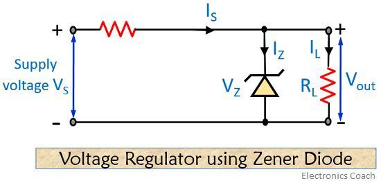
Let’s have a look at the circuit diagram of voltage regulator employing Zener diode-
A Zener diode is used as a voltage regulator that provides a constant voltage from a source whose voltage varies substantially.

As we can see in the figure shown above, a resistor is placed at the beginning of the circuit. In order to limit the reverse current through the diode to a safer value resistor, Rs is employed in the circuit.
The source voltage Vs and resistor Rs are so selected that the diode operates in the breakdown region. The voltage across RL is known as Zener voltage Vz and diode current is known as Iz.
A steady state voltage is maintained across the load RL, as the output voltage fluctuations get absorbed by the resistor Rs. The input voltage whose changes are to be regulated connects the Zener diode in reverse condition.
The diode does not conduct unless the voltage across RL is less than Zener diode breakdown voltage Vz, and Rs and RL constitute a potential divider across Vs.
As the supply voltage Vs is increased, in this case, the voltage drop across RL will be more as compared to the Zener diode breakdown voltage. Thus, causing Zener diode to conduct in its breakdown region.
The Zener current Iz is limited by the series resistor Rs from exceeding rated max value Izmax.
Current through RS is given by- Source current gets split into Iz and IL at the junction-
![]()
The voltage across Zener diode Vz remains constant until it is operating in breakdown region through the Zener current ID may vary considerably.
If here, the input voltage is increased further, the current through the diode and load increases. As the resistance across the diode decreases this will cause more current to flow through the diode.
As a result, the voltage drop across Rs will be more thus the voltage at the output will be a value that is close to the input or supply voltage.
Hence we can say, the Zener diode maintains a uniform voltage across the load unless the supply voltage is more than Zener voltage.
Discrete Transistor Voltage Regulator
When we talk about transistor voltage regulator it is basically of 2 types –
By the use of any of the above-mentioned types, we can have a constant dc output voltage of a predetermined value. This value is independent of the variation in supply voltage or load at the output.
Let’s now discuss each type in detail-
Series Voltage Regulator
The figure below shows the block diagram of the series voltage regulator-
Here, the magnitude of input that gets output voltage is controlled by the series control elements. The circuit that samples output voltage provides feedback that is compared with the reference voltage.
In case if the voltage at the output increases, comparator sends the control signal to the control element so as to reduce the magnitude of the output. Similarly, if the output voltage decreases, comparator sends control signal so that the magnitude of output can be raised to the desired level.
Working of the transistor series voltage regulator
It is also known as an emitter follower voltage regulator. The circuit below shows a simple series voltage regulator that is formed using an NPN transistor and Zener diode.
In the above circuit, the collector and emitter terminals of the transistor are in series with the load that’s why it is called series regulator. The transistor Q is known as the series pass transistor.
When dc supply is given to the input terminal it causes the regulated output voltage to appear across the load resistor RL. The transistor employed in the circuit serves as variable resistance and Zener diode supplies the reference voltage.
Its operation is based on the principle that a large variation in input appears across the transistor thus output voltage tends to be constant.
Here, Vout = Vz – VBE
The base voltage remains almost constant whose value is somewhat equal to the voltage across the Zener diode Vz.
Moving further and let us consider the case where the output voltage is increased due to increase in the supply voltage. This increase in Vout will resultantly decrease VBE as Vz is fixed at a certain level.
This reduction in VBE will automatically reduce the conduction. Due to this, collector-emitter resistance RCE increases, thus causing VCE to increase, ultimately output voltage gets reduced.
Now, what about the effect of the change in load at the output voltage.
Suppose the value of load resistor RL decreases thus causing the current through it to increase. In such a condition, Vout starts decreasing due to which VBE increases. Ultimately, the conduction level of transistor increases that decreases the RCE.
This decrease in the resistance increases the current slightly that compensates for the reduction in RL.
Thus the output voltage remains constant as it is equal to ILRL.
Limitations
- At room temperature, maintaining an absolutely constant output voltage is difficult because as the room temperature rises up, automatically it will cause reduction in VBE and VZ.
- Good regulation is not obtained at high current.
Shunt Voltage Regulator
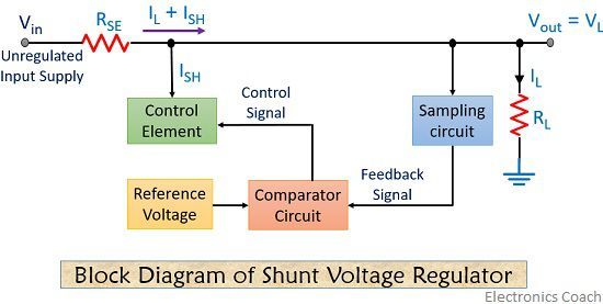
The block diagram of shunt voltage regulator is shown below-
In this type of voltage regulator, in order to provide adequate regulation, the current is shunted away from the load. To maintain the constant current, by making use of control element some current is shunted away from the load.
Suppose there is a change in load, thus causing the output voltage to change. So, a feedback signal is sent to the comparator circuit that provides the control signal to vary the magnitude of current shunted away from the load.
Working of transistor shunt voltage regulator
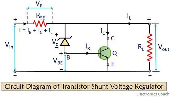
Let’s have a look at the circuit diagram of the shunt voltage regulator-
Here, RSE is connected in series with supply and the transistor is connected across the output. The supply voltage reduces due to drop across RSE, this reduction in voltage depends on the current supplies to RL.
Vout = Vz + VBE
Vout= Vin – IRSE
Suppose, the input voltage is increased thus causing the rise in Vout and VBE resultantly causing the increase in IB and IC. So, with this increase in supply voltage, supply current I increase, that creates more voltage drop across RSE thus reducing output voltage. Thus output voltage remains almost constant.
Limitations
- It causes a large portion of the current to flow through the transistor rather than to load.
- Overvoltage protection is sometimes a problem in these type of circuits.
Applications
These are used in computer power supplies where they regulate dc voltage. In power distribution system, voltage regulators are used along distribution lines so as to provide the constant voltage to the consumers.
Innocent says
your explanation is best