As we are aware of the fact that a time base generator does not provide accurate linearity in sweep voltages. Thus various methods of Sweep Voltage Generation are used in order to have a linear output.
The methods are discussed below:
Exponential sweep circuit
The circuit of a basic sawtooth voltage generator is shown below: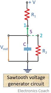
In the circuit, the position of switch S changes from 1 to 2 thus causing the capacitor to be charged and discharged alternately. Thus an output is achieved that is shown below:
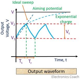
Here, Ts and Tr are the sweep and retrace time respectively. The display systems require to retrace time so that the started beam can return to its initial position before the beginning of the next cycle.
When the switch is at position 1, the capacitor charges with the supply voltage V. But, before it is fully charged the switch changes its position to 2 that causes the capacitor to discharge until the switch does not return to position 1 again. Thus we can have an output as shown above. The supply voltage potential is also termed as aiming potential.
The voltage at the output is given by:
![]()
and
![]()
When t = Ts, Vout (Ts) = V2
![]()
Furthermore, at t = Tr, Vout(Tr) = V1
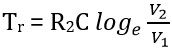
Vs is the sweep amplitude and is given by![]()
As we can see in the waveform that the straight line and exponential charges are nearly identical in case of a smaller value of V2. So, in order to achieve better linearity, the sweep voltage must be a small portion of a supply voltage.
Now, moving further let us consider, switching circuit comprising of a UJT.
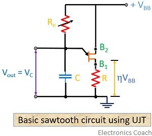
Here, the capacitor employed in the circuit is charged through resistor Re when VBB is in on state.
At the time of capacitor charging, there is an exponential increase in the voltage across the capacitor before attaining peak potential Vp. As the capacitor attains peak value during charging, the UJT switches on that cause the capacitor to discharge quickly via B1. When the voltage across R increases, the voltage across the capacitor drops to Vv. This causes the device to cut off and again the charging of the capacitor starts. In this way, a continuous process generates a sawtooth waveform and the resulting waveform is shown below.
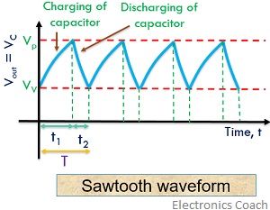
As the time constant is dependent on resistor Re. So, the frequency of the output can be varied according to the variation in Re. In normal conditions, t2 is very much less than t1 and can be neglected for approximate calculations.
At the time of charging, the capacitor voltage is given by,
![]()
: ReC= τ i.e., the time constant
As we know, after the charging period, when Vp becomes equal to Vc the capacitor starts to discharge.
![]()
![]() It can be written as,
It can be written as,![]()
when VB is neglected.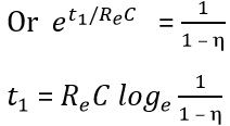
Therefore, the charging period,
Seeing that, discharging time is small as compared to charging time.
Hence, T = t1
The time period of the wave is given as,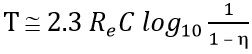
And the frequency of oscillation is given as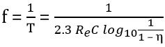
Turn ON and OFF condition of a UJT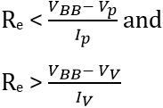
So, we can write,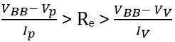
Bootstrap time base generator
In this category in order to maintain a constant current, bootstrapping is done.
What is bootstrapping?
It is basically a process in which by using a feedback system, some part of the output is given back to the input, thereby increasing or decreasing the input impedance of the circuit.
As we can see in the figure shown below:
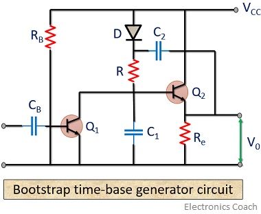
It consists of two transistors Q1 and Q2 along with a diode D. The anode side of the diode is connected to VCC and the cathode side is connected to the output capacitor C2. The output voltage is observed as the voltage across capacitor C1 employed in the circuit.
Operation:
At time t = 0, Vcc drives the circuit, that turns on Q1. The capacitor C2 employed in the circuit is charged to Vcc through the diode. A negative trigger pulse applied at the base of Q1 turns it off. This causes C2 to discharge and now C1 starts charging. Due to large capacitance value, C2 discharges slowly thereby maintaining a constant value.
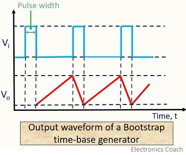
Now, the diode D is reverse biased at ramp time. A small amount of current is provided by C2 to C1 in order to charge it. At the end of ramp time when Q1 gets on, the charged capacitor C1 now discharges and the voltage appears across the output. Again when D gets forward biased C2 recovers its charge lost at the time of charging C1. Thus the circuit produces a ramp output that is shown below:
Miller sweep generator
It is also known as miller integrator that generates a sweep waveform. The initial stage of a miller circuit comprised of a switch along with a timing circuit as shown in the figure below:
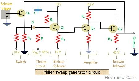
The rest part of the circuit serves as an amplifier section and emitter follower section works as a buffer amplifier having high input impedance and low output impedance. This resultantly provides higher amplifier gain. The sweep speed of the generator varies with the variation in R, C and VBB.
Operation:
Here, transistor Q4 turns on by the application of the negative pulse from the output of the Schmitt trigger. Thus current flows through resistor R1. This negative potential forward biases the diode in the circuit but as C is the bypass capacitor here so it will not be charged.
When the trigger is applied, it causes Q4 to turn off. The switch employed in the circuit applies a potential of 10 V that causes current to flow through R1 thus making the diode reverse biased. The applied VBB potential now charges the capacitor through resistor R and generates a sweep signal at the output. At the end of the sweep, the capacitor discharges through D and Q4.
Leave a Reply