A diode is a two-terminal device formed by placing a layer of P-type semiconductor next to N -type semiconductor. It forms a P-N Junction. The interface which joins both is made up of metal. Thus, it is referred as a metallurgical junction.
A diode is a controlling element for electronic devices and circuits.
Rectifiers, Amplifiers, linear and digital Integrated circuits, switching circuits, etc. are controlled with the help of diode.

P-N Junction
The P-type Semiconductor has mobile holes and immobile negative acceptor ions. On the contrary, the N-type material has mobile electrons and immobile positive ions. The holes, as well as electrons, are uniformly distributed in P-type and N-type material respectively. When P-N Junction forms, electrons from an N-type material, tend to diffuse into the P-type material. Similarly, holes in the P-type material will tend to diffuse into the N-type material.
Diffusion Current
The diffusion happens due to density gradient. The density of electrons is higher in N-type material and lower in P-type. Thus, it diffuses from N-type to P-type across the junction. The density of holes in the P-type material is more than in N-type material. Thus, they diffuse from P-type material to N-type material across the junction.
Due to this movement, some of the electrons and holes combine at the junction. This process is known as diffusion, and the current produced due to diffusion is called diffusion current.
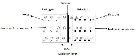
The current produced due to diffusion is limited. At a particular time, this diffusion current stops. It happens because after a particular time electrons stop diffusing into the P-type material and holes stop diffusing into the N-type material.
I will explain the reason behind this phenomenon later in this article. When electrons and holes diffuse they combine at the junction due to which the junction is depleted of mobile charge carriers.
Depletion layer
The area which is depleted of mobile charge carriers is called depletion layer. The width of the depletion layer is 10-6m. Thus, the negative potential is developed across the P-type material, and a positive potential is developed across the N-type material. Now, when electrons try to diffuse into a P-type material, they will feel repulsion from negative potential developed across the P-type material.
When holes try to diffuse into N-type material they will be repelled from +ve potential developed across the N-type material. Therefore after a particular time, no more electrons and holes can diffuse across the junction due to barrier potential. Thus, initial diffusion of charge carriers creates barrier potential at the junction. The value of barrier potential in case of Germanium is 0.3V and in the case of Silicon, it is 0.7V.

Factors Affecting Barrier Potential
Barrier Potential is affected by various factors such as doping density, electric charge and temperature. Doping density and electric charge depend on the type of material. Thus, it is fixed for a particular junction. But temperature variation causes variation in barrier potential.
The junction temperature is the temperature of junction inside the diode and the temperature outside the diode is ambient temperature. When diode conducts the junction temperature increases and it is higher than ambient temperature. The heat is dissipated by the recombination of electron and holes.
With the increase in junction temperature, more electron and holes combine, and it reduces the width of the depletion layer. When the depletion layer’s width decreases the barrier potential also decreases. Thus, with the increase in junction temperature the magnitude of barrier potential decreases.
Diode Biasing
When an external voltage source is applied to P-N junction diode, it is called diode biasing.
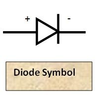
P-N Junction diode is a device which conducts when it is forward biased and does not conduct when it is reverse biased. But this is possible only in case of an ideal diode. Practical diodes do not conduct instantly when forward biased and do not stop conducting instantly when it is reverse biased; it produces leakage current. Let’s discuss this two types of biasing in detail.
Forward Biasing
When the +ve terminal of the external voltage is connected to a P-type semiconductor, and the negative terminal of the battery is connected to the N-type semiconductor, it is called forward biasing. The mechanism of current flow in forward biasing of a diode can be understood with the help of these points mentioned below:-
(i) When the positive terminal of battery source is connected to a P-type section of a diode, the holes in the P-type semiconductor are repelled from the +ve terminal of the battery. These holes when repelled from the +ve terminal, they tend to move towards the junction.
(ii) Electrons in N-type semiconductor get attracted towards positive terminal of the battery, and they also tend to move towards the junction. Thus, electrons and holes moving towards junction recombine at the junction.
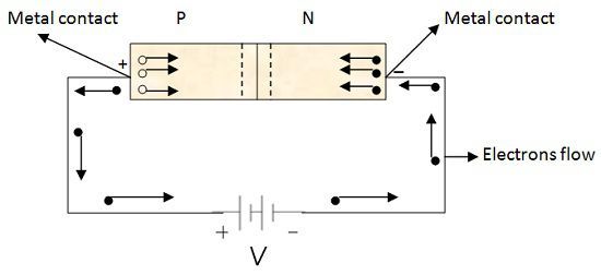
(iii) When this electron-hole recombination takes place the junction temperature increase. Due to increase in junction temperature, more electron and holes recombine as a consequence of which width of depletion layer reduces.
(iv) The reduction in depletion layer results in the reduction of barrier potential. In this way, forward current starts flowing in a P-N junction diode. This current is due to the movement of majority charge carriers.The value of barrier potential in case of Germanium (0.3V) and Silicon (0.7V) is too small.
Reverse Biasing
When -ve terminal of the battery is connected to a P-type semiconductor, and the +ve terminal of the battery is connected to the N-type material then it is called reverse biasing of a diode. The mechanism of reverse diode biasing can be understood with the help of these points mentioned below:-
(i) When negative terminal of the battery is connected to the P-type semiconductor, the holes in the P-type semiconductor will be attracted towards -ve terminal of the battery. On the other hand, electrons in the N-type material will be attracted towards positive terminal of the battery.
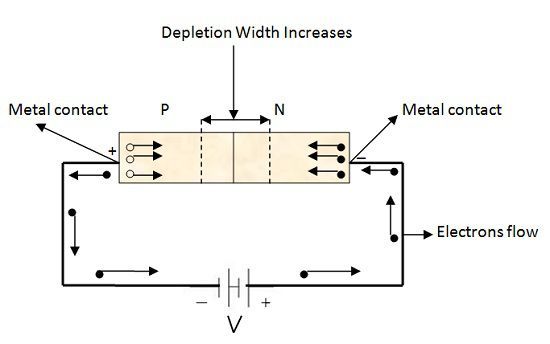
(ii) In this way, majority charge carriers in both P-type and N-type material will move away from the junction. As a consequence of which the width of depletion layer starts increasing.
(iii) With the increase of the width of the depletion region, the barrier potential also starts increasing. Thus, reverse biasing of diode increases the barrier potential.
(iv) The junction will offer higher resistance and diode will not conduct. Only a small amount of leakage current will flow in reverse diode.
Leakage Current or Reverse Saturation Current
The diode does not conduct in reverse biasing, but a small amount of leakage current flows in reverse biasing. This is because of minority charge carriers. When the depletion layers start increasing majority charge carriers cannot cross the junction.
On the contrary, minority charge carriers i.e. electrons in P-type and holes in N-type flow across the junction the junction. The current due to this minority charge carriers is called leakage current. But leakage current does not depend on reverse voltage.
But leakage current does not depend on reverse voltage. On the contrary, the reverse current is dependent on temperature. With the increase of temperature more covalent bonds break and more minority charge carriers generate due to which reverse saturation current increases.
Ideal Diode
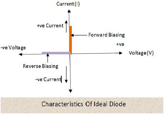
The diode which starts conducting instantly on forward biasing and stops conducting instantly on reversed biased. The ideal diode acts as a conductor when it is forward biased. On the contrary, it acts as an insulator when it is reverse biased. Practically, it is not possible.
Practical Diode
Practically, diode does not start conducting instantly. It begins conducting when it crosses barrier potential. And on reverse biased it does not become an insulator.
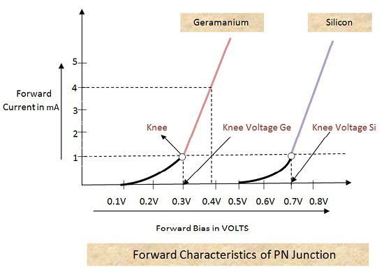
Knee Voltage: The forward voltage, at which the current through the junction starts increasing rapidly is called knee voltage or cut-in voltage. In the case of Germanium the value of knee voltage is 0.3V, and in the case of silicon, it is 0.7V which is too low.
A small amount of forward voltage is sufficient to eliminate the effect of barrier potential. Thus, with the reduction of barrier potential, the resistance in the path of current reduces and forward current starts flowing in the circuit.
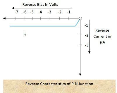
Practically, when the diode is reversed biased the potential barrier increases, due to which junction resistance increases. There is no possibility of current due to majority charge carriers. A small amount of current flows due to minority charge carriers. It is called leakage current.
The value of leakage current increases with reverse voltage but after a certain time, it becomes constant. Thus, any further increase in reverse voltage will not contribute to leakage current. Thus, it is also called reverse saturation current.
The value of reverse saturation current depends on temperature. The reverse current (I0) approximately gets double for each 100 C rise in temperature in the case of Germanium and each 80C rise in temperature in the case of silicon.
Leave a Reply