There are mainly two types of Photodiode i.e. PIN Photodiode and Avalanche Photodiode.
PIN Photodiode
Definition: PIN Photodiode is a photodetector in which the depletion layer thickness can be modified for generation of large photocurrent. If the thickness of depletion layer is more then the surface area on which light is falling also increases. Due to this, the conversion efficiency of a photodiode increases and more photocurrent will generate.
Construction of PIN Photodiode
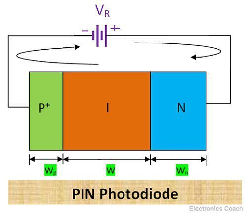
The P-type layer, intrinsic layer and N-type layer are sandwiched to form two junctions NI junction and PI junction. The P+ layer can be obtained by ion implantation and the intrinsic layer is an epitaxial layer grown on N-type substrate. The electrons from N-side and holes from P-side diffuse due to the concentration gradient.

The depletion region is formed. The width of the depletion region is more in intrinsic region and it is narrow in the N-type layer. The P-type terminal is connected to negative terminal of battery and N-type terminal is connected to positive terminal of the battery.
Working of PIN Photodiode
When the reverse bias is applied to PIN diode the width of depletion region starts increasing in the intrinsic region. And with the increase of reverse voltage, the width increases even more. The stage is reached when the depletion region’s width becomes equivalent to the thickness of the intrinsic layer. In this point, the intrinsic layer is swept free of mobile charge carriers.

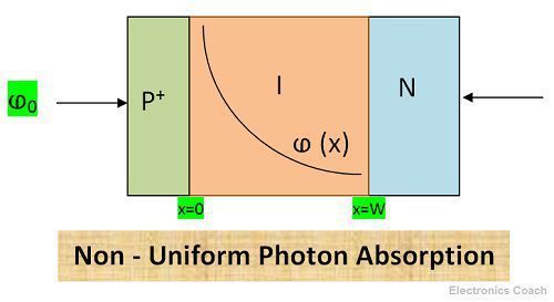
Consider a photon flux ⱷ0 is incident on P+ region of the diode and width of P+ region is very small in comparison to intrinsic and N – type layer. The photon flux can be defined as a function of distance.
ⱷ(x) = ⱷ0e–αx
Here α is the photon absorption coefficient, x varies with the width of the intrinsic layer. The density of photocurrent generated due to photon flux can be given by below equation.
JL = e Wƪ 0 GL dx = e Wƪ 0 ⱷ0 e-αx dx = eⱷ0 (1 – e–αW)
Here JL is photocurrent density, GL is the generation rate of electron hole pair from the edges of the intrinsic layer. In the above equation, it is assumed that there is no electron-hole recombination within the depletion region i.e. it is completely free of mobile charge carriers. And each photon absorbed generates one electron-hole pair.
Advantages and Disadvantages of PIN Photodiode
- The advantage is its high-frequency response and its frequency response is also greater than Cadmium – Sulphide photodetector.
- It is inexpensive and the response time is in nanoseconds which make it appropriate for electronic circuitry.
- These diodes have a broad spectral response and they can process even very weak signals.
- The disadvantage of PIN diode is that it requires large reverse bias for its operation which sometimes reduces the signal to noise ratio.
Applications of PIN Photodiode
They are used for detection of laser pulses, in ultrafast switching circuits and in logic circuits due to their ability to detect weak signals.
Avalanche Photodiode
Definition: Avalanche photodiode is a photodetector in which more electron-hole pairs are generated due to impact ionisation. It is like P-N photodiode or PIN photodiode where electron-hole pairs are generated due to absorption of photons but in addition to this avalanche photodiode uses the impact ionisation principle for increasing magnitude of photocurrent.
Construction of Avalanche Photodiode
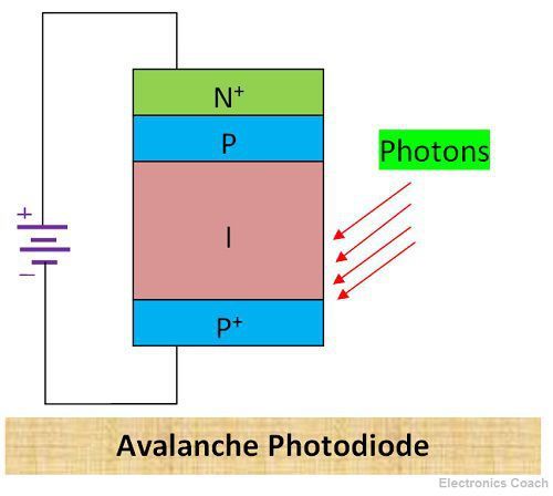
It has four regions N+ region, P region, an intrinsic layer and P+ region. The N+ and P+ region are heavily doped and the intrinsic layer is lightly doped. Its construction can be understood more clearly with the help of the below diagram.

Working of Avalanche Photodiode
We have already discussed in Photodiodes and PIN Photodiodes that photons striking the surface of diodes contribute to the photocurrent. But in the case of avalanche diode, an additional factor is introduced to impact ionisation which increases photocurrent several times. This additional factor is called avalanche multiplication factor.
Impact ionisation is the process in which one energy carrier with sufficient high kinetic energy strikes bounded energy carrier and imparts its energy to it so that the bounded energy carrier can move freely. This leads to higher concentration of energy carriers and thus higher magnitude of current.
This phenomenon of impact implantation plays a significant role in increasing photocurrent. The current – gain bandwidth product of Avalanche photodiode is about 100 GHz. Thus, this type of photodiode can respond to light modulated at microwave frequencies.
Advantages and Disadvantages of Avalanche Photodiode
- It can detect very weak signal due to high current-gain bandwidth product.
- The construction is quite complicated i.e. care should be taken about the junction. The junction should be uniform and the guard ring is used to protect the diode from edge breakdown.
Applications of Avalanche photodiode
Due to its ability to detect low-level signals it is used in fibre optic communication Systems. A properly designed silicon avalanche photodiode can provide a response time of about 1ns.
Leave a Reply