Definition: Logic gates are basically electronic circuits that perform logical functions such as addition, subtraction, multiplication etc. For any digital system, it acts as an elemental building block and is able to make logical decisions.
It performs logical functions in order to produce an output when two or more inputs are applied. Basically, the operation of logic gates is represented by algebraic expressions.
To form a big logic network sometimes, the output of a gate is fed to the input of other. Logic gates operate on binary logic 0 and 1 where 0 indicates low and 1 indicates a high voltage level.
The basic logic gates are OR, AND, NOT. However, there exist some universal logic gates such as NAND and NOR. Combination of several logic gates, allows us to perform a very complicated logic function in any complex circuitry.
The various input-output possibilities for a logic circuit is expressed with the help of a truth table. In other words, truth table shows variation in output with respect to the input.
Now, let us move further and have a look at how various gates perform the logic operation.
OR logic gate
The OR logic gate is used to perform addition of the applied input signals. It produces high output for one or more than one high input and symbolically denoted by plus sign (+).
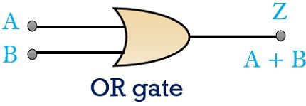
The output expression for OR gate is given as-
Z = A + B
The figure below shows the circuit diagram of OR gate consisting of diodes 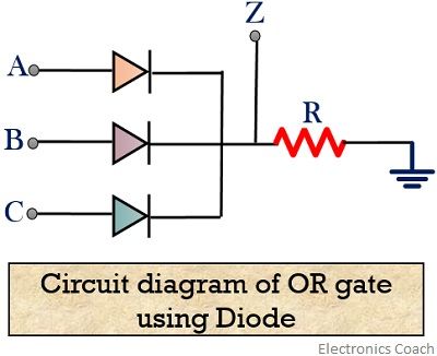
As we know, that diode conducts in a forward biased condition. So, when a high voltage is applied at any of the input terminals, the corresponding diode gets forward biased.
Thus allowing current to flow through the circuit, resultantly providing the high voltage at the output.
Similarly, when a low voltage is applied, the diode gets reverse biased. Thus, no current flows through the diode that corresponds to that particular terminal.
Let us now separately discuss 2, 3 and multiple input condition of OR gate.
- 2 input OR gate:
As we have already mentioned that logic high is achieved in case of OR gate when one or more than one input is high. Otherwise, the output is low.
The figure below shows the logic symbol for two input OR gate:
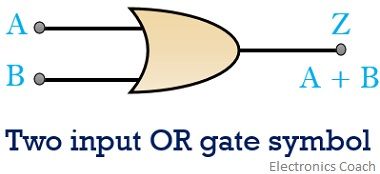
The truth table for OR gate is shown below:
| A | B | Z |
|---|---|---|
| 0 | 0 | 0 |
| 0 | 1 | 1 |
| 1 | 0 | 1 |
| 1 | 1 | 1 |
Let’s understand the operation of OR gate by considering various cases:
Case 1: When both the applied input is low i.e., 0, the output generated is also low. This is because the summation of the low voltage signal produces a low voltage at its output.
Case 2: When the voltage applied at terminal A is 0 and at terminal B is 1 i.e., logic high then after summation the OR gate produces high value at its output.
Case 3: When logic low i.e., 0 is applied to terminal B and the logic high is applied to terminal A. Then, the summation of the two values produces a logic high at the output.
Case 4: When a high-level signal is applied to both the terminals of the gate then their summation produces logic 1 at its output.
- 3 input OR gate:
The logic symbol for a 3 input OR gate is shown below: 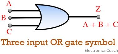
The logical operation of the gate is described with the help of the truth table shown below:
| A | B | C | Z |
|---|---|---|---|
| 0 | 0 | 0 | 0 |
| 0 | 0 | 1 | 1 |
| 0 | 1 | 0 | 1 |
| 0 | 1 | 1 | 1 |
| 1 | 0 | 0 | 1 |
| 1 | 0 | 1 | 1 |
| 1 | 1 | 0 | 1 |
| 1 | 1 | 1 | 1 |
One can also construct multiple input OR gate. Let us consider an OR gate consisting of 6 inputs.
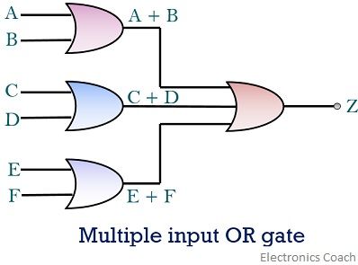
So, the Boolean expression is given as
Z = (A+B) + (C+D) + (E+F)
OR gate using transistor
The figure here shows the transistor OR gate circuit that contains 3 transistors Q1, Q2 and Q3 having common supply voltage Vcc = + 5V.
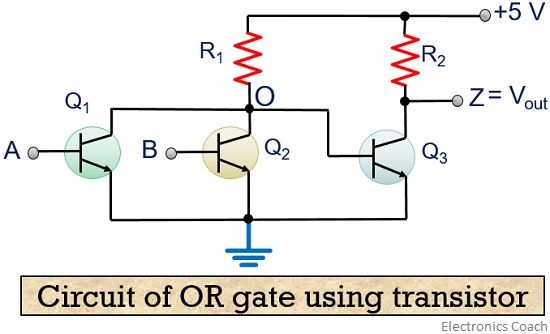
Here, Q1 gets forward biased when +5 V is applied at terminal A. At the saturation point of Q1, the supply voltage is dropped across R1 that causes O to go to ground. Resultantly, Q3 gets cut-off that causes output Z to go to Vcc = 5V. Thus, producing a high output.
Suppose when both terminals A and B is supplied with a low voltage, then O drives to + 5V as Q1 and Q3 gets cut-off. This allows Q3 to conduct fully due to forward biasing and + 5v potential drops across R2 that leads to low voltage at the output.
Pinout configuration for 2 input OR gate:
The figure here shows the pin-out configuration of IC 7432 for 2 input OR gate.
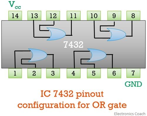
It consists of 14 pins dual in-line package having four, 2 input OR gate.
Sometimes input in the form of pulses is provided to an OR gate whose output is the result of the various combination of input.
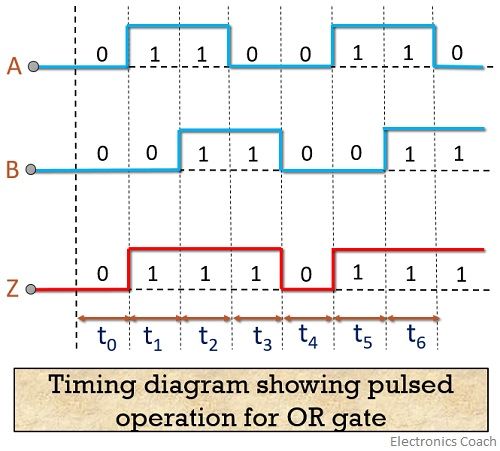
We can see here, a timing diagram for OR gate that depicts two input pulses A and B along with an output Z.
Here, at to, both the inputs are low, thus produces a low output. But, at t1 when the input of A is high and B is low, the output produced is also high. Similarly, at t2 when input at A is low and input at B is high then another high voltage level is achieved at the output.
At time interval t4, both the inputs are at a high voltage level then the output corresponding to that interval is also high.
Thus we can say OR gate basically performs the addition operation.
AND logic gate
The AND gate executes multiplication of the applied input signal and produces a single output. A high output for the AND gate is achieved only when both the applied inputs are high otherwise the output is low.
As it performs the multiplication operation, thus symbolically expressed as a single dot (.)
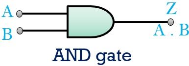
The output expression for the AND gate is given by:
Z = A.B
The figure here shows the circuit of AND gate consisting of diodes: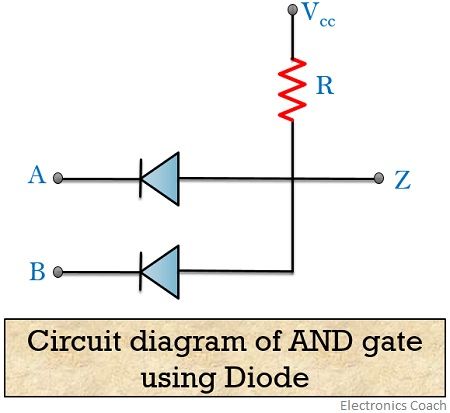
Here, the supply voltage Vcc of + 5V is common and the two terminal A and B is provided with either low or high voltages in various combinations.
Let us consider that either A or B terminal is applied with a low voltage, in such a condition, the corresponding diode will become forward biased. Thus causing current to flow through it.
Due to this, the whole 5V potential is dropped across R which resultantly causes the low voltage at output Z. The same condition is applicable when both the terminals are at a low voltage level.
When terminal A and B both are at the high potential the this causes the diode to get reverse biased. Hence the diodes corresponding to both the terminals get off and doesn’t conduct.
Thus no current flows through R hence supply voltage appears at the output. Resultantly logic high is obtained at Z.
Moving further let us now discuss 2, 3 and multiple input condition for AND gate:
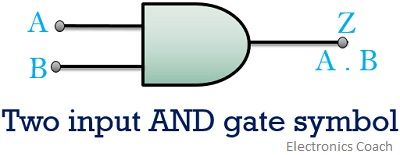
2 input AND gate:
The logical symbol for AND gate consisting of 2 inputs is shown below:
The respective truth table for AND gate is shown below:
| A | B | Z |
|---|---|---|
| 0 | 0 | 0 |
| 0 | 1 | 0 |
| 1 | 0 | 0 |
| 1 | 1 | 1 |
Consider the following cases in order to understand the truth table of AND gate:
Case 1: When a low-level voltage is applied at both the terminals of the gate then due to multiplication function the result obtained is also low i.e., 0.
Case 2: When terminal A is fed with low voltage level but B is fed with high voltage level then the output produced will definitely be low. This is so because the product of 0 and 1 will surely provide 0 as output.
Case 3: Another condition arises when terminal A is kept at high potential however, B is kept at a low potential. In such a condition output will be low due to product rule.
Case 4: When terminal A and B both kept at high potential then the multiplication function causes the output to be high. This is because the product of 1 and 1 will provide the output as also 1.
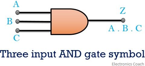
3 input AND gate
The figure below shows the logic symbol for 3 inputs:
3 input logical AND operation can be clearly understood with the help of the truth table shown below:
| A | B | C | Z |
|---|---|---|---|
| 0 | 0 | 0 | 0 |
| 0 | 0 | 1 | 0 |
| 0 | 1 | 0 | 0 |
| 0 | 1 | 1 | 0 |
| 1 | 0 | 0 | 0 |
| 1 | 0 | 1 | 0 |
| 1 | 1 | 0 | 0 |
| 1 | 1 | 1 | 1 |
AND gate consisting of multiple can also be constructed. The figure here shows 6 inputs applied to the AND gate:
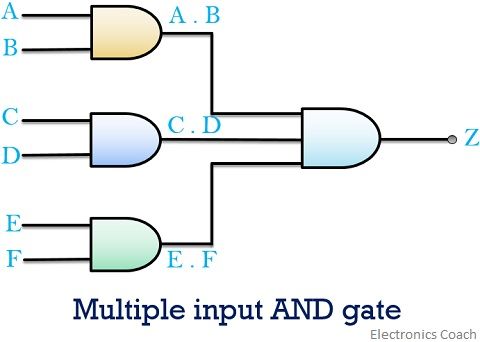
The Boolean expression for 6 input AND gate is given as:
Z = (A.B).(C.D).(E.F)
AND gate using transistor
The figure represents a transistor AND gate circuit:
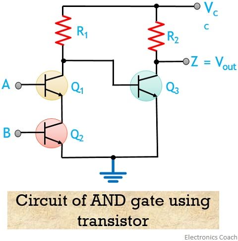
Let us consider first that low potential is provided to both the terminals. This causes Q1 and Q2 to get cut-off thus no any voltage drop will be there at R1.
Thus, a potential at Q3 causes it to become forward biased and it starts conducting. The voltage provided at the input will get dropped across R2, hence at the output logic 0 is obtained. The same output is obtained when any of the two applied input terminals is low.
When the two transistors are provided with the logic high then both of them starts conducting. The current produced drops the supply voltage at R1. Hence Q3 gets cut-off causing +5v to appear across the output. Thus, logic high is obtained at the output when terminals A and B are fed with high voltage level.
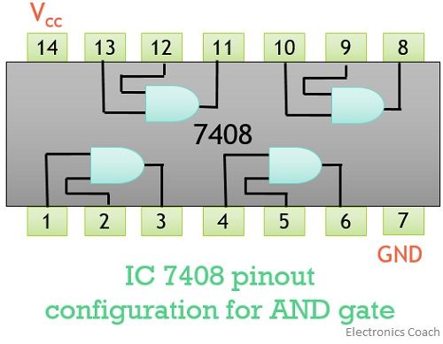
Pinout configuration of 2 input AND gate
The figure below shows the pinout diagram of IC 7408, 2 input AND gate.
For pulsed input the timing diagram is shown below:
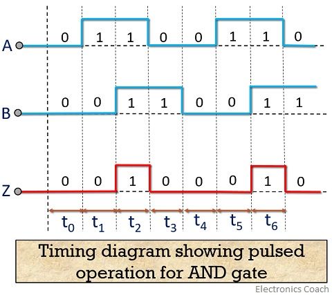
As we can see here, that when both the applied pulses at the two terminals is high then only the output will be high otherwise low-level signal is obtained at the output.
NOT logic gate
NOT logic circuits basically perform inversion function when employed in any circuit. It is based on single input single output logic and is also known as an inverter.
It basically produces high output for low input and a low output for the high input. Or we can say, any input logic level is changed to its opposite level by using an inverter.
The symbolic representation of NOT gate is shown below:
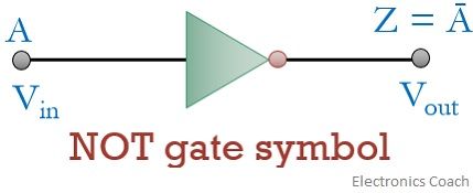
Here, bubble in the symbol indicates complement of input at the output.
The logic equation for the inverter is given below:
Z = NOT A
= Ā
The truth table for NOT gate is shown below:
| A | Z |
|---|---|
| 0 | 1 |
| 1 | 0 |
When the applied input is 0 or low the output produced is 1 or high. Similarly, for high applied input, the output achieved is low this is how an inverter works.
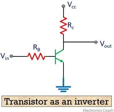
Transistor as an inverter:
The figure below shows the application of the transistor as an inverter.
Let’s now see how this happens-
When a low-level voltage is applied at the input then it causes transistor current to be 0, then at the output potential is equivalent to supply voltage + 5V.
On the contrary when the high voltage level is applied at the input then current flows through the transistor. This flow of current will cause a voltage drop across Rc thus low voltage level is obtained at the output.
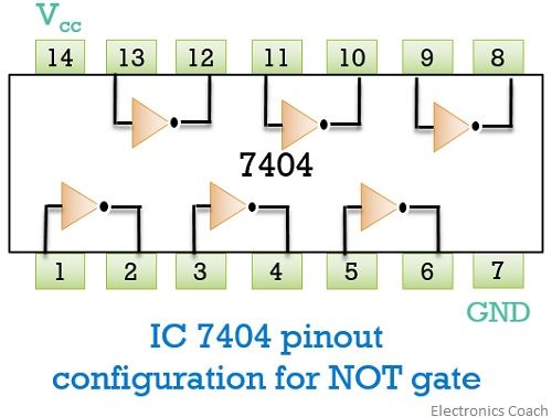
Pinout configuration for NOT gate
The figure shows the pinout configuration of IC 7404 for inversion.
In the case of pulsed input, when the low input pulse is applied then output achieved is high. However, when the high input pulse is applied then it inverts the input and produces logic low at the output. As we can see in the figure shown below:
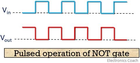
Thus we can say that an inverter on operation produces an inverted signal at the output.
Shashi Gupta says
It is very useful form me😄
Thanks 🤗
Adnan Anam says
Thanks a lot for such a simple explanation. One can easily refer for such beautiful explanation
Paul Elai says
Precise