Definition: Voltage Source Inverter abbreviated as VSI is a type of inverter circuits that converts a dc input voltage into its ac equivalent at the output. It is also known as a voltage-fed inverter (VFI), the dc source at the input of which has small or negligible impedance.
In a VSI, battery banks are considered to be the simplest form of dc voltage source which is a combination of multiple cells in series and parallel combinations. However, sometimes photovoltaic cells are also used as a dc source of supply. Sometimes, the primary source to the circuit can be an ac supply source so, in that case, first, the ac signal must be converted into dc, and then the dc signal will be given to the inverter to get the ac equivalent of dc voltage.
It is to be noted here that the actually attained ac output signal may or may not be equivalent to the magnitude and frequency of the actual ac input signal.
What is an Inverter?
An inverter in the field of power electronics is basically power conversion circuits that are defined as the circuits that change dc power into ac equivalent of desired voltage as well as frequency. These have enormous applications such as in UPS, induction heating, HVDC transmission lines, adjustable speed ac drives, etc. It performs the inverse operation of ac to dc converter, thus, it is called so.
There are two major classifications of the inverter, namely, voltage source inverter and current source inverter. Voltage source inverter changes the dc form of voltage into ac form, likewise a current source inverter changes dc form of current into ac form. The current source inverter is sometimes called the current fed inverter, in this case, the input terminal has a stiff dc current source in the case of the dc voltage source.
We have already discussed while discussing commutation that when devices get turned off by the application of negative gate pulse then it is known as self-commutation. So, in voltage source inverters, if GTO is used then to turn it off negative gate current pulse will be required. While sometimes, transistors like BJT, MOSFET, etc. when used in VSI then these get turned off by controlling the base current.
Single-phase Bridge Inverters
According to the orientation or connection of semiconductor devices to form inverter circuits, the inverters are classified as:
- Bridge Inverters
- Series Inverters
- Parallel Inverters
Out of the above three types, bridge inverters are quite popular and are used majorly. Thus, here we will discuss the bridge orientation of voltage source inverters.
Half-Bridge Inverter
The figure given below shows the circuit representation of a single-phase half-bridge inverter:
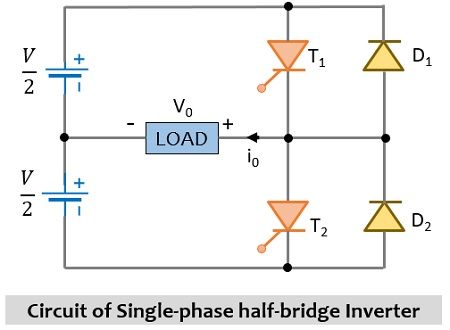
As we can see that the above circuit consists of thyristors and diodes along with the dc power input source. Here an initial assumption is made that the thyristor connected in the circuit conducts only till the time, the gate pulse is present across it and as soon as the gate pulse is removed it gets commutated. For this circuit, we have considered that at time instant T/2 the gate pulse from one thyristor is removed and immediately provided to another thyristor in the given configuration. Thus, this makes the two thyristors conduct one after the other and not simultaneously.
Thus, we can say that the whole circuit operation is divided into two periods:
Period I: 0 ≤ t ≥ T/2; T1 is conducting
Period II: T/2 ≤ t ≥ T; T2 is conducting
This means that at instant T/2, a gate pulse is removed from T1 and applied to T2. The figure given below represents the waveform representation of single-phase half-bridge inverter:
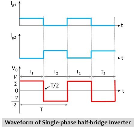
The circuit operation is such that for a time duration between 0 to T/2, T1 is in conducting state due to the supply input V/2. This allows current Ig1 to flow through the load for this particular condition. Thus, in the above-given waveform representation, a square wave is shown for the period between 0 to T/2.
Moreover, when at T/2 instant gate pulse is removed from T1 and applied to T2, the T2 begins to conduct. But this time, the voltage across the load will be –V/2 due to the lower potential of voltage V/2. In this case, current Ig2 will flow through the load. Thus, for the time duration between T/2 to T, square wave representation is shown above. However, as we can see clearly, for T2 the waveform is in opposite direction to that of T1 and the reason for this is the opposite direction of flow of current.
Hence, in this way, square wave ac output voltage is obtained. And by varying the time instant for application and removal of gate pulse the frequency of this ac signal can be varied.
The operation of a half-bridge inverter makes use of 3 wire dc supply which was a major drawback hence to overcome this full-bridge inverter was considered.
Full-Bridge Inverter
The figure below represents the circuit diagram of a single-phase full-bridge inverter:
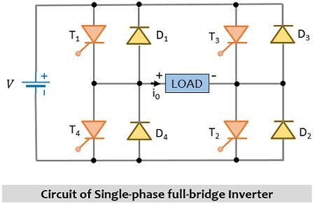
It is clearly shown in the above figure that there are four thyristors and four diodes in the configuration. This means here the number of thyristors and diodes is twice of the count of the half-bridge inverter.
The circuit operation takes place in a way that, for a time duration between 0 to T/2, thyristors T1 and T2 are triggered by gate pulse thus the two conduct and the load voltage will be V i.e., equivalent to the supply input. While for time instant between T/2 to T, thyristors T3 and T4 begin to conduct as gate pulse is removed from T1 and T2 and provided to T3 and T4 at instant T/2.
The waveform representation is shown below:
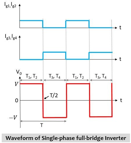
The operation is similar to that of a half-bridge inverter but the difference here is that the amplitude of output voltage is double in this case than the previous case.
Steady-state Analysis
For half-bridge inverter, the load voltage is given as:
For full-bridge inverter, the load voltage will be:

The current flowing through the load shows dependency upon the nature of the load. So, suppose the load is RLC, then the voltage equation for half-bridge inverter for 0 < t < T/2
![]()
: Vc1 represents the initial voltage across the capacitor of the RLC load at t=0.
In a similar way, we can write the equation for a full-bridge inverter by replacing V/2 from V.
The voltage equation for half-bridge inverter for T/2 < t’ < T,
![]()
: Vc2 represents the initial voltage across load capacitor at t’ = 0.
Likewise, for the full-bridge rectifier here we can replace –V/2 by –V.
On differentiating the above two equations, we will have,
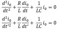
Thus, we can say that the components of the load lead to cause variation in load current waveform.
Leave a Reply