Definition: A power diode or high-power diode is one of the power semiconductor devices that have two terminals (cathode and anode) similar to the normal PN junction diode but exhibit higher power handling capability. These are designed to handle several kiloamps of current in forward biased condition with negligible power loss and must block several kilovolts under reverse-biased state.
More simply, we can say that power diodes are devices that are designed to carry a large amount of current at high voltage. Power semiconductor devices mainly find their use in power electronic circuits.
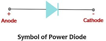
Symbolically a power diode is represented as:
Before elaborating more about power diodes, it is important to recall-
What is a Diode?
A normal diode is a low-power diode that has a PN junction and is also known as a signal diode. We have already discussed in our previous content on diodes that a diode offers unidirectional flow of current. It is a combination of p and n-type semiconductor materials that conduct when forward biased and block the flow of current when reverse biased.
A power diode also has a PN junction that permits the flow of current in a single direction only. But it differs from that of a low-power diode in terms of its construction and the features offered. From features here we mean the enhanced level of voltage, current, and power ratings provided by high power diodes. Also, unlike signal diodes, these operate at lower switching speeds.
Basics of PN junction
The fundamental entity that is responsible for the operation of various power semiconductor devices is a p-n junction. Even in signal diodes, we have seen that a p-n junction is formed by physical contact between p and n-type semiconductor materials.
We are already familiar with the basics that p-type has majority holes and minority electrons while n-type has majority electrons and minority holes. However, to form power diodes variation in concentration of p and n types of materials is required. A p-type material can be denoted as p+, p, and p-, and n-type can be designated as n+, n, and n– according to variation in doping concentration.
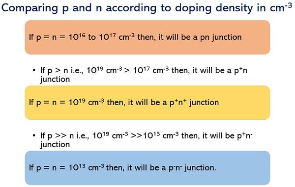
Thus, in general, we can conclude p+ as a highly doped p region and n– as a lightly doped n region.
Need for Power Diodes?
Basically, the signal diodes are used in low-power rectification circuits. However, in all such applications where large forward-biased current and high reverse-biased blocking voltage are needed, the small-signal diodes do not perform well. This is so because signal diodes are not constructionally built to handle such a large current so in case a large current is provided then they will be overheated resulting in destroying the device.
Thus, to overcome the drawbacks of signal diodes, power diodes came into existence.
Now, the question arises how does it do so?
A power diode offers a comparatively larger p-n junction region than a signal diode. Thus, it offers a high forward current capability that ranges several hundred amps and a large value of blocking the reverse voltage i.e., up to several thousand volts.
Construction of Power Diodes
We have already discussed that a power diode is constructed in a different manner to that of the signal diode. A signal diode simply has a PN junction. But for the suitability of power diodes towards high voltage and current applications, it is constructed in a quite complex manner.
The constructional structure of power diodes is shown below:
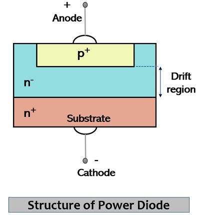
An n+ heavily doped substrate is considered over which epitaxially an n– layer is grown, moreover, diffusion of p+ layer takes place over the n– region. This p+ region forms the anode connection while the n+ substrate forms the cathode connection.
While discussing the p-n junction diode we have seen that no such structure was present there. Thus, here p+ and n+ regions are anode and cathode respectively while the n– region acts as a drift region. In the reverse biased condition, the depletion region gets absorbed within the drift region. The thickness of the n– region and the breakdown voltage of the diode in reverse biased show direct proportionality with each other.
Thus, the wider the n– region, the more will be the breakdown voltage.
However, in forward conduction mode, the n– region sum ups for the ohmic resistance to the diode. This leads to large power dissipation and to deal with this, cooling arrangements are to be necessarily made.
Working of Power Diodes
The way power diodes operate is somewhat similar to that of normal diodes. Consider the forward biased condition of a power diode shown below, where the positive terminal of the battery is connected to the anode and the negative terminal forms a connection with the cathode.
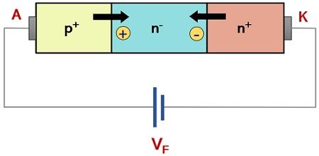 In this condition, junction J1 will get forward biased and majority carriers (holes) from the p+ region start injecting into the n- drift region. When the injection rate is low then the holes of the p+ region will recombine with electrons of the n– region. But as the injection rate is increased then holes will penetrate and recombine with electrons of the n+ region. This is called double injection. Due to this flow of carriers and recombination within the drift region, the diode starts conducting heavily once the threshold is surpassed.
Now, consider the reverse biased condition, where the negative terminal of the battery forms a connection with the anode and the positive terminal is connected to the cathode.
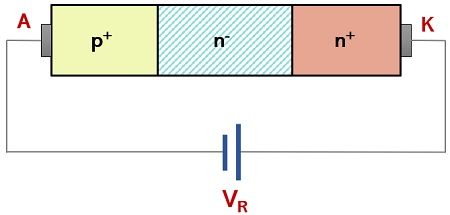 In this condition, the junction becomes reverse biased and like a normal diode, power diode also stops conduction in this condition. Here the depletion region is extended up to the drift region that will cause difficulty for the minority carriers to penetrate the junction and recombine.
But it is to be noted here that a sudden change in polarity of applied potential will not immediately stop the flow of current. Moreover, the minority charges stored in the junction will lead to the flow of small leakage current (of order 100 mA) through the diode in opposite direction. This reverse current shows dependency on variation in junction temperature.
Once the applied potential becomes equal to the breakdown voltage, then impact ionization will take place.
What is impact ionization?
The reverse applied voltage excites the electric field due to which the electrons will get accelerated. After gaining sufficient kinetic energy, the moving electrons may be able to liberate more electrons from the covalent bonds of silicon atoms. This cumulative process generates a large number of free electrons due to which large reverse current flows through the device.
This large reverse current considerably increases the power dissipation hence may lead to destroying the diode. Thus, it is said that the operation of the device in the reverse breakdown region must be avoided.
I-V Characteristics
Initially with no supply voltage forward current is 0 but as the supply input increases, and reaches the threshold value (of about 0.7 V), a small amount of forward current flows through the device. Once the threshold value is surpassed, a considerable increase in diode current (at 1V) is noticed as it starts conduction. Here linear rise in forward current is noticed when voltage increases beyond the threshold.
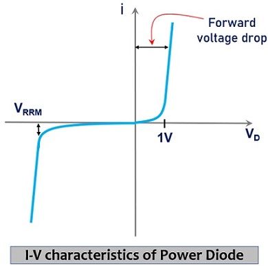
In reverse biased mode, leakage current flows through the device which is independent of the applied potential but once breakdown is achieved then even at approximately constant voltage, a high amount of reverse current flows.
Reverse Recovery Characteristics
As we have discussed recently even after removal of forward applied voltage, the diode conducts due to stored charge in the depletion region and the semiconductor layer. So, the time being for which this leakage current flows is called reverse recovery time, trr. The blocking ability of the diode is regained till the time the leakage current becomes 0.
The trr is the time between the moment forward current vanishes and the moment the reverse recovery current remains only 25% of its peak value IRM.
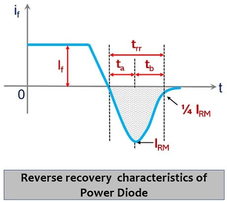
From the figure, it is clear that
trr = ta + tb
: ta is the interval between zero crossings of forward current and peak reverse current IRM. During ta the charge within the depletion region, is vanished. While tb is the duration from the peak of reverse current IRM to 0.25% IRM. During tb, the charge from the layers of semiconductors is removed.
The ratio of tb and ta is termed as softness factor given by S. It is generally unity, hence such diode with S equal to 1 is called soft recovery diode. While if S>1 hence it is called fast recovery or snappy recovery diode.
Types of Power Diode
The classification of power diodes is done on the basis of reverse recovery characteristics possessed by them.
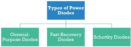
- General Purpose Diodes: These possess trr quite high i.e., of about 25 microseconds. Low-frequency applications such as rectification, converters operated nearly up to 1KHz uses this diode. Its current rating lies between 1 A to several thousand amperes and its voltage rating lies between 50 V to 5 KV.
- Fast Recovery Diodes: These exhibit trr quite low i.e., of about 5 microseconds. Mainly used in electrical power conversion systems. Its current rating lies between 1 A to several thousand amperes and its voltage rating lies between 50 V to 3 KV.
- Schottky Diodes: In these diodes instead of p-n junction, metal-semiconductor junction is formed where generally aluminium is preferred for metal and silicon for semiconductor. Its current rating lies between 1 A to 300 A while the reverse voltage rating is about 100 V.
Applications
Due to the characteristics of power diodes, these are mainly used as freewheeling diodes, in ac to dc and dc to ac conversion systems, rectification, battery charging, etc. Along with these, power diodes are also used in electroplating, UPS, choppers, SMPS, and induction heating as well.
Leave a Reply